- 您现在的位置:买卖IC网 > PDF目录9713 > AD7843ARUZ-REEL7 (Analog Devices Inc)IC ADC 12BIT TOUCHSCREEN 16TSSOP PDF资料下载
参数资料
| 型号: | AD7843ARUZ-REEL7 |
| 厂商: | Analog Devices Inc |
| 文件页数: | 6/21页 |
| 文件大小: | 0K |
| 描述: | IC ADC 12BIT TOUCHSCREEN 16TSSOP |
| 标准包装: | 1,000 |
| 类型: | 电阻 |
| 触摸面板接口: | 4 线 |
| 输入数/键: | 1 TSC |
| 分辨率(位): | 12 b |
| 评估套件: | 可供 |
| 数据接口: | 串行 |
| 数据速率/采样率 (SPS,BPS): | 125k |
| 电压基准: | 外部 |
| 电源电压: | 2.2 V ~ 5.25 V |
| 工作温度: | -40°C ~ 85°C |
| 安装类型: | 表面贴装 |
| 封装/外壳: | 16-TSSOP(0.173",4.40mm 宽) |
| 供应商设备封装: | 16-TSSOP |
| 包装: | 带卷 (TR) |
| 配用: | EVAL-AD7843EBZ-ND - BOARD EVAL FOR AD7843 |
AD7843
Rev. B | Page 13 of 20
Touch Screen Settling
In some applications, external capacitors could be required
across the touch screen to filter noise associated with it, for
example, noise generated by the LCD panel or backlight
circuitry. The value of these capacitors causes a settling time
requirement when the panel is touched. The settling time
typically appears as a gain error. There are several methods for
minimizing or eliminating this issue. The problem could be that
the input signal, reference, or both have not settled to their final
value before the sampling instant of the ADC. Additionally, the
reference voltage could still be changing during the conversion
cycle. One option is to stop, or slow down the DCLK for the
required touch screen settling time. This allows the input and
reference to stabilize for the acquisition time, which resolves the
issue for both single-ended and differential modes.
The other option is to operate the AD7843 in differential mode
only for the touch screen and to program the AD7843 to keep
the touch screen drivers on and not go into power-down (PD0
= PD1 = 1). Several conversions might be required, depending
on the settling time required and the AD7843 data rate. Once
the required number of conversions are made, the AD7843 can
then be placed into a power-down state on the last
measurement. The last method is to use the 15 DCLK cycle
mode, which maintains the touch screen drivers on until it is
commanded to stop by the processor.
Reference Input
The voltage difference between +REF and REF (see Figure 19)
sets the analog input range. The AD7843 operates with a refer-
ence input in the range of 1 V to VCC. The voltage into the VREF
input is not buffered and directly drives the capacitor DAC
portion of the AD7843. Figure 20 shows the reference input
circuitry. Typically, the input current is 8 A with VREF = 2.5 V
and fSAMPLE = 125 kHz. This value varies by a few microamps,
depending on the result of the conversion. The reference current
diminishes directly with both conversion rate and reference
voltage. As the current from the reference is drawn on each bit
decision, clocking the converter more quickly during a given
conversion period does not reduce the overall current drain
from the reference.
02144-
B
-020
X+
Y+
VREF
3-TO-1
MUX
ADC
Figure 20. Reference Input Circuitry
When making touch screen measurements, conversions can be
made in the differential (ratiometric) mode or the single-ended
mode. If the SER/DFR bit is set to 1 in the control register, a
single-ended conversion is performed. Figure 21 shows the
configuration for a single-ended Y-coordinate measurement.
The X+ input is connected to the analog to digital converter, the
Y+ and Y drivers are turned on, and the voltage on X+ is
digitized. The conversion is performed with the ADC referenced
from GND to VREF. The advantage of this mode is that the
switches that supply the external touch screen can be turned off
once the acquisition is complete, resulting in a power saving.
However, the on resistance of the Y drivers affects the input
voltage that can be acquired. The full touch screen resistance
may be in the order of 200 to 900 , depending on the manu-
facturer. Therefore if the on resistance of the switches is
approximately 6 , true full-scale and zero-scale voltages cannot
be acquired regardless of where the pen/stylus is on the touch
screen. Note that the minimum touch screen resistance
recommended for use with the AD7843 is approximately 70 .
02144-
B
-021
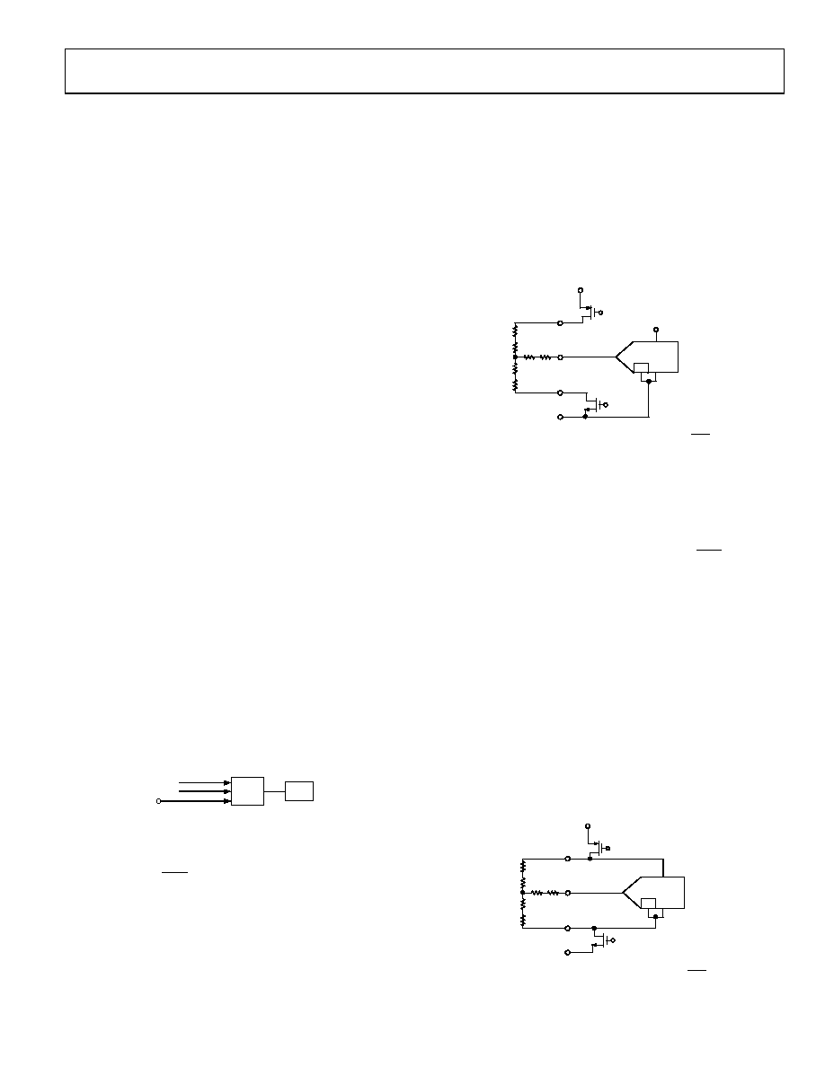
+VCC
VREF
GND
Y+
Y–
X+
IN+
IN–
REF+
ADC CORE
REF–
Figure 21. Single-Ended Reference Mode (SER/DFR = 1)
In this mode of operation, therefore, some voltage is likely to be
lost across the internal switches and, in addition to this, it is
unlikely that the internal switch resistance will track the resis-
tance of the touch screen over temperature and supply, providing
an additional source of error.
The alternative to this situation is to set the SER/DFR bit low. If
one again considers making a Y-coordinate measurement, but
now the +REF and REF nodes of the ADC are connected
directly to the Y+ and Y pins, this means the analog-to-digital
conversion is ratiometric. The result of the conversion is always
a percentage of the external resistance, independent of how it
could change with respect to the on resistance of the internal
switches. Figure 22 shows the configuration for a ratiometric Y-
coordinate measurement. It should be noted that the differential
reference mode can be used only with +VCC since the source of
the +REF voltage and cannot be used with VREF.
The disadvantage of this mode of operation is that during both
the acquisition phase and conversion process, the external touch
screen must remain powered. This results in additional supply
current for the duration of the conversion.
02144-
B
-022
+VCC
GND
Y+
Y–
X+
IN+
IN–
REF+
ADC CORE
REF–
Figure 22. Differential Reference Mode (SER/DFR = 0)
相关PDF资料 |
PDF描述 |
|---|---|
| VE-24F-IW-B1 | CONVERTER MOD DC/DC 72V 100W |
| VI-JWK-MX-F1 | CONVERTER MOD DC/DC 40V 75W |
| VE-24B-IW-B1 | CONVERTER MOD DC/DC 95V 100W |
| VI-BTM-IV-B1 | CONVERTER MOD DC/DC 10V 150W |
| AD7843ARQZ-REEL7 | IC ADC 12BIT TOUCHSCREEN 16-QSOP |
相关代理商/技术参数 |
参数描述 |
|---|---|
| AD7845 | 制造商:AD 制造商全称:Analog Devices 功能描述:LC2MOS Complete 12-Bit Multiplying DAC |
| AD7845AQ | 功能描述:IC DAC 12BIT MULT LC2MOS 24-CDIP RoHS:否 类别:集成电路 (IC) >> 数据采集 - 数模转换器 系列:- 产品培训模块:Data Converter Fundamentals DAC Architectures 标准包装:750 系列:- 设置时间:7µs 位数:16 数据接口:并联 转换器数目:1 电压电源:双 ± 功率耗散(最大):100mW 工作温度:0°C ~ 70°C 安装类型:表面贴装 封装/外壳:28-LCC(J 形引线) 供应商设备封装:28-PLCC(11.51x11.51) 包装:带卷 (TR) 输出数目和类型:1 电压,单极;1 电压,双极 采样率(每秒):143k |
| AD7845AR | 制造商:Rochester Electronics LLC 功能描述:12-BIT PARALLEL VOUT DAC, IC - Bulk 制造商:Analog Devices 功能描述: |
| AD7845ARZ | 功能描述:IC DAC 12BIT MULT LC2MOS 24SOIC RoHS:是 类别:集成电路 (IC) >> 数据采集 - 数模转换器 系列:- 产品培训模块:Data Converter Fundamentals DAC Architectures 标准包装:750 系列:- 设置时间:7µs 位数:16 数据接口:并联 转换器数目:1 电压电源:双 ± 功率耗散(最大):100mW 工作温度:0°C ~ 70°C 安装类型:表面贴装 封装/外壳:28-LCC(J 形引线) 供应商设备封装:28-PLCC(11.51x11.51) 包装:带卷 (TR) 输出数目和类型:1 电压,单极;1 电压,双极 采样率(每秒):143k |
| AD7845BQ | 功能描述:IC DAC 12BIT MULT LC2MOS 24-CDIP RoHS:否 类别:集成电路 (IC) >> 数据采集 - 数模转换器 系列:- 产品培训模块:Data Converter Fundamentals DAC Architectures 标准包装:750 系列:- 设置时间:7µs 位数:16 数据接口:并联 转换器数目:1 电压电源:双 ± 功率耗散(最大):100mW 工作温度:0°C ~ 70°C 安装类型:表面贴装 封装/外壳:28-LCC(J 形引线) 供应商设备封装:28-PLCC(11.51x11.51) 包装:带卷 (TR) 输出数目和类型:1 电压,单极;1 电压,双极 采样率(每秒):143k |
发布紧急采购,3分钟左右您将得到回复。