- 您现在的位置:买卖IC网 > PDF目录10806 > AD7845JN (Analog Devices Inc)IC DAC 12BIT MULTIPLYING 24-DIP PDF资料下载
参数资料
| 型号: | AD7845JN |
| 厂商: | Analog Devices Inc |
| 文件页数: | 10/12页 |
| 文件大小: | 0K |
| 描述: | IC DAC 12BIT MULTIPLYING 24-DIP |
| 产品培训模块: | Data Converter Fundamentals DAC Architectures |
| 产品变化通告: | Product Discontinuance 27/Oct/2011 |
| 标准包装: | 15 |
| 设置时间: | 5µs |
| 位数: | 12 |
| 数据接口: | 并联 |
| 转换器数目: | 1 |
| 电压电源: | 双 ± |
| 功率耗散(最大): | 150mW |
| 工作温度: | 0°C ~ 70°C |
| 安装类型: | 通孔 |
| 封装/外壳: | 24-DIP(0.300",7.62mm) |
| 供应商设备封装: | 24-PDIP |
| 包装: | 管件 |
| 输出数目和类型: | 1 电压,单极;1 电压,双极 |
| 采样率(每秒): | 200k |
AD7845
REV. B
–7–
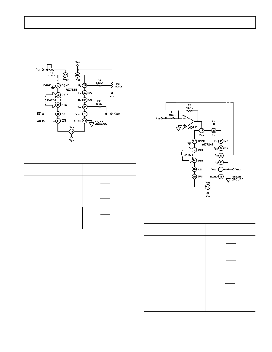
UNIPOLAR BINARY OPERATION
Figure 13 shows the AD7845 connected for unipolar binary
operation. When VIN is an ac signal, the circuit performs
2-quadrant multiplication. The code table for Figure 13 is given
in Table I.
Figure 13. Unipolar Binary Operation
Table I. Unipolar Binary Code Table for AD7845
Binary Number In
DAC Register
Analog Output, VOUT
MSB
LSB
1111
–VIN
4095
4096
1000
0000
–VIN
2048
4096
= –1/2 VIN
0000
0001
–VIN
1
4096
0000
0 V
OFFSET AND GAIN ADJUSTMENT FOR FIGURE 13
Zero Offset Adjustment
1. Load DAC with all 0s.
2. Trim R3 until VOUT = 0 V.
Gain Adjustment
1. Load DAC with all 1s.
2. Trim R1 so that VOUT = –VIN
4095
4096
.
In fixed reference applications, full scale can also be adjusted by
omitting R1 and R2 and trimming the reference voltage magni-
tude. For high temperature applications, resistors and potenti-
ometers should have a low temperature coefficient.
BIPOLAR OPERATION
(4-QUADRANT MULTIPLICATION)
The recommended circuit for bipolar operation is shown in
Figure 14. Offset binary coding is used.
The offset specification of this circuit is determined by the
matching of internal resistors RB and RC and by the zero code
offset error of the device. Gain error may be adjusted by varying
the ratio of R1 and R2.
To use this circuit without trimming and keep within the gain
error specifications, resistors R1 and R2 should be ratio
matched to 0.01%.
The code table for Figure 14 is given in Table II.
Figure 14. Bipolar Offset Binary Operation
Table II. Bipolar Code Table for Offset Binary Circuit of
Figure 14
Binary Number In
DAC Register
Analog Output, VOUT
MSB
LSB
1111
+VIN
2047
2048
1000
0000
0001
+VIN
1
2048
1000
0000
0 V
0111
1111
–VIN
1
2048
0000
–VIN
2048
= –VIN
相关PDF资料 |
PDF描述 |
|---|---|
| LTC2851IMS8#PBF | IC TXRX RS485/RS422 8MSOP |
| LM393WDT | IC COMPARATOR DUAL 0.4MA 8-SOIC |
| VI-B4F-IV-S | CONVERTER MOD DC/DC 72V 150W |
| AD7948BR | IC DAC 12BIT MULTIPLYING 20-SOIC |
| LTC2852IMS#PBF | IC TXRX RS485/RS422 10MSOP |
相关代理商/技术参数 |
参数描述 |
|---|---|
| AD7845JN | 制造商:Analog Devices 功能描述:SEMICONDUCTORSLINEAR |
| AD7845JNZ | 功能描述:IC DAC 12BIT MULT LC2MOS 24-DIP RoHS:是 类别:集成电路 (IC) >> 数据采集 - 数模转换器 系列:- 产品培训模块:Lead (SnPb) Finish for COTS Obsolescence Mitigation Program 标准包装:50 系列:- 设置时间:4µs 位数:12 数据接口:串行 转换器数目:2 电压电源:单电源 功率耗散(最大):- 工作温度:-40°C ~ 85°C 安装类型:表面贴装 封装/外壳:8-TSSOP,8-MSOP(0.118",3.00mm 宽) 供应商设备封装:8-uMAX 包装:管件 输出数目和类型:2 电压,单极 采样率(每秒):* 产品目录页面:1398 (CN2011-ZH PDF) |
| AD7845JP | 功能描述:IC DAC 12BIT MULT LC2MOS 28-PLCC RoHS:否 类别:集成电路 (IC) >> 数据采集 - 数模转换器 系列:- 标准包装:2,400 系列:- 设置时间:- 位数:18 数据接口:串行 转换器数目:3 电压电源:模拟和数字 功率耗散(最大):- 工作温度:-40°C ~ 85°C 安装类型:表面贴装 封装/外壳:36-TFBGA 供应商设备封装:36-TFBGA 包装:带卷 (TR) 输出数目和类型:* 采样率(每秒):* |
| AD7845JP-REEL | 功能描述:Bit Digital to Analog Converter 28-PLCC (11.51x11.51) 制造商:analog devices inc. 系列:* 包装:带卷(TR) 零件状态:上次购买时间 位数:* 数模转换器数:* 建立时间:* 输出类型:* 差分输出:* 数据接口:* 参考类型:* 电压 - 电源,模拟:* 电压 - 电源,数字:* INL/DNL(LSB):* 架构:* 工作温度:* 封装/外壳:28-LCC(J 形引线) 供应商器件封装:28-PLCC(11.51x11.51) 标准包装:1 |
| AD7845JPZ | 功能描述:IC DAC 12BIT MULT LC2MOS 28-PLCC RoHS:是 类别:集成电路 (IC) >> 数据采集 - 数模转换器 系列:- 标准包装:1 系列:- 设置时间:4.5µs 位数:12 数据接口:串行,SPI? 转换器数目:1 电压电源:单电源 功率耗散(最大):- 工作温度:-40°C ~ 125°C 安装类型:表面贴装 封装/外壳:8-SOIC(0.154",3.90mm 宽) 供应商设备封装:8-SOICN 包装:剪切带 (CT) 输出数目和类型:1 电压,单极;1 电压,双极 采样率(每秒):* 其它名称:MCP4921T-E/SNCTMCP4921T-E/SNRCTMCP4921T-E/SNRCT-ND |
发布紧急采购,3分钟左右您将得到回复。