- 您现在的位置:买卖IC网 > PDF目录10806 > AD7845JN (Analog Devices Inc)IC DAC 12BIT MULTIPLYING 24-DIP PDF资料下载
参数资料
| 型号: | AD7845JN |
| 厂商: | Analog Devices Inc |
| 文件页数: | 7/12页 |
| 文件大小: | 0K |
| 描述: | IC DAC 12BIT MULTIPLYING 24-DIP |
| 产品培训模块: | Data Converter Fundamentals DAC Architectures |
| 产品变化通告: | Product Discontinuance 27/Oct/2011 |
| 标准包装: | 15 |
| 设置时间: | 5µs |
| 位数: | 12 |
| 数据接口: | 并联 |
| 转换器数目: | 1 |
| 电压电源: | 双 ± |
| 功率耗散(最大): | 150mW |
| 工作温度: | 0°C ~ 70°C |
| 安装类型: | 通孔 |
| 封装/外壳: | 24-DIP(0.300",7.62mm) |
| 供应商设备封装: | 24-PDIP |
| 包装: | 管件 |
| 输出数目和类型: | 1 电压,单极;1 电压,双极 |
| 采样率(每秒): | 200k |
AD7845
REV. B
–4–
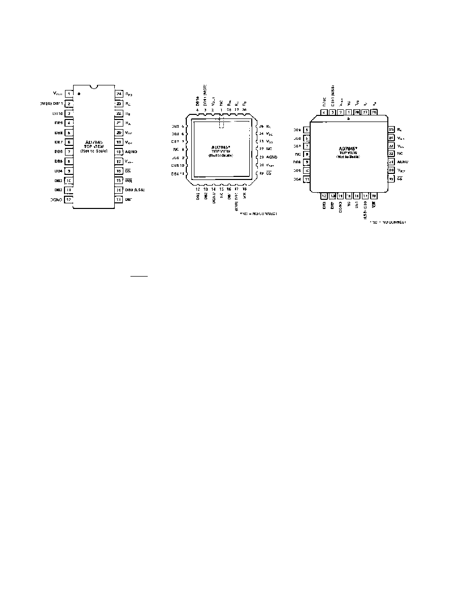
PIN CONFIGURATIONS
LCC
PLCC
DIP, SOIC
DIGITAL-TO-ANALOG GLITCH IMPULSE
This is the amount of charge injected from the digital inputs to
the analog output when the inputs change state. This is nor-
mally specified as the area of the glitch in either pA-secs or
nV-secs depending upon whether the glitch is measured as a
current or voltage. The measurement takes place with VREF =
AGND.
DIGITAL FEEDTHROUGH
When the DAC is not selected (i.e.,
CS is high) high frequency
logic activity on the device digital inputs is capacitively coupled
through the device to show up as noise on the VOUT pin. This
noise is digital feedthrough.
MULTIPLYING FEEDTHROUGH ERROR
This is ac error due to capacitive feedthrough from the VREF
terminal to VOUT when the DAC is loaded with all 0s.
OPEN-LOOP GAIN
Open-loop gain is defined as the ratio of a change of output
voltage to the voltage applied at the VREF pin with all 1s loaded
in the DAC. It is specified at dc.
UNITY GAIN SMALL SIGNAL BANDWIDTH
This is the frequency at which the magnitude of the small signal
voltage gain of the output amplifier is 3 dB below unity. The
device is operated as a closed-loop unity gain inverter (i.e.,
DAC is loaded with all 1s).
OUTPUT RESISTANCE
This is the effective output source resistance.
FULL POWER BANDWIDTH
Full power bandwidth is specified as the maximum frequency, at
unity closed-loop gain, for which a sinusoidal input signal will
produce full output at rated load without exceeding a distortion
level of 3%.
TERMINOLOGY
LEAST SIGNIFICANT BIT
This is the analog weighting of 1 bit of the digital word in a
DAC. For the AD7845, 1 LSB =
V
REF
2
12
.
RELATIVE ACCURACY
Relative accuracy or endpoint nonlinearity is a measure of the
maximum deviation from a straight line passing through the
endpoints of the DAC transfer function. It is measured after
adjusting for both endpoints (i.e., offset and gain error are ad-
justed out) and is normally expressed in least significant bits or
as a percentage of full-scale range.
DIFFERENTIAL NONLINEARITY
Differential nonlinearity is the difference between the measured
change and the ideal 1 LSB change between any two adjacent
codes. A specified differential nonlinearity of +1 LSB max over
the operating temperature range ensures monotonicity.
GAIN ERROR
Gain error is a measure of the output error between an ideal
DAC and the actual device output with all 1s loaded after offset
error has been adjusted out. Gain error is adjustable to zero
with an external potentiometer. See Figure 13.
ZERO CODE OFFSET ERROR
This is the error present at the device output with all 0s loaded
in the DAC. It is due to the op amp input offset voltage and
bias current and the DAC leakage current.
TOTAL HARMONIC DISTORTION
This is the ratio of the root-mean-square (rms) sum of the har-
monics to the fundamental, expressed in dBs.
OUTPUT NOISE
This is the noise due to the white noise of the DAC and the
input noise of the amplifier.
相关PDF资料 |
PDF描述 |
|---|---|
| LTC2851IMS8#PBF | IC TXRX RS485/RS422 8MSOP |
| LM393WDT | IC COMPARATOR DUAL 0.4MA 8-SOIC |
| VI-B4F-IV-S | CONVERTER MOD DC/DC 72V 150W |
| AD7948BR | IC DAC 12BIT MULTIPLYING 20-SOIC |
| LTC2852IMS#PBF | IC TXRX RS485/RS422 10MSOP |
相关代理商/技术参数 |
参数描述 |
|---|---|
| AD7845JN | 制造商:Analog Devices 功能描述:SEMICONDUCTORSLINEAR |
| AD7845JNZ | 功能描述:IC DAC 12BIT MULT LC2MOS 24-DIP RoHS:是 类别:集成电路 (IC) >> 数据采集 - 数模转换器 系列:- 产品培训模块:Lead (SnPb) Finish for COTS Obsolescence Mitigation Program 标准包装:50 系列:- 设置时间:4µs 位数:12 数据接口:串行 转换器数目:2 电压电源:单电源 功率耗散(最大):- 工作温度:-40°C ~ 85°C 安装类型:表面贴装 封装/外壳:8-TSSOP,8-MSOP(0.118",3.00mm 宽) 供应商设备封装:8-uMAX 包装:管件 输出数目和类型:2 电压,单极 采样率(每秒):* 产品目录页面:1398 (CN2011-ZH PDF) |
| AD7845JP | 功能描述:IC DAC 12BIT MULT LC2MOS 28-PLCC RoHS:否 类别:集成电路 (IC) >> 数据采集 - 数模转换器 系列:- 标准包装:2,400 系列:- 设置时间:- 位数:18 数据接口:串行 转换器数目:3 电压电源:模拟和数字 功率耗散(最大):- 工作温度:-40°C ~ 85°C 安装类型:表面贴装 封装/外壳:36-TFBGA 供应商设备封装:36-TFBGA 包装:带卷 (TR) 输出数目和类型:* 采样率(每秒):* |
| AD7845JP-REEL | 功能描述:Bit Digital to Analog Converter 28-PLCC (11.51x11.51) 制造商:analog devices inc. 系列:* 包装:带卷(TR) 零件状态:上次购买时间 位数:* 数模转换器数:* 建立时间:* 输出类型:* 差分输出:* 数据接口:* 参考类型:* 电压 - 电源,模拟:* 电压 - 电源,数字:* INL/DNL(LSB):* 架构:* 工作温度:* 封装/外壳:28-LCC(J 形引线) 供应商器件封装:28-PLCC(11.51x11.51) 标准包装:1 |
| AD7845JPZ | 功能描述:IC DAC 12BIT MULT LC2MOS 28-PLCC RoHS:是 类别:集成电路 (IC) >> 数据采集 - 数模转换器 系列:- 标准包装:1 系列:- 设置时间:4.5µs 位数:12 数据接口:串行,SPI? 转换器数目:1 电压电源:单电源 功率耗散(最大):- 工作温度:-40°C ~ 125°C 安装类型:表面贴装 封装/外壳:8-SOIC(0.154",3.90mm 宽) 供应商设备封装:8-SOICN 包装:剪切带 (CT) 输出数目和类型:1 电压,单极;1 电压,双极 采样率(每秒):* 其它名称:MCP4921T-E/SNCTMCP4921T-E/SNRCTMCP4921T-E/SNRCT-ND |
发布紧急采购,3分钟左右您将得到回复。