参数资料
| 型号: | AD7847BRZ |
| 厂商: | Analog Devices Inc |
| 文件页数: | 12/12页 |
| 文件大小: | 0K |
| 描述: | IC DAC 12BIT DUAL MULT 24-SOIC |
| 产品培训模块: | Data Converter Fundamentals DAC Architectures |
| 标准包装: | 1 |
| 设置时间: | 4µs |
| 位数: | 12 |
| 数据接口: | 并联 |
| 转换器数目: | 2 |
| 电压电源: | 双 ± |
| 工作温度: | -40°C ~ 85°C |
| 安装类型: | 表面贴装 |
| 封装/外壳: | 24-SOIC(0.295",7.50mm 宽) |
| 供应商设备封装: | 24-SOIC W |
| 包装: | 管件 |
| 输出数目和类型: | 2 电压,单极;2 电压,双极 |
| 采样率(每秒): | 250k |
AD7837/AD7847
REV. C
–9–
APPLICATIONS
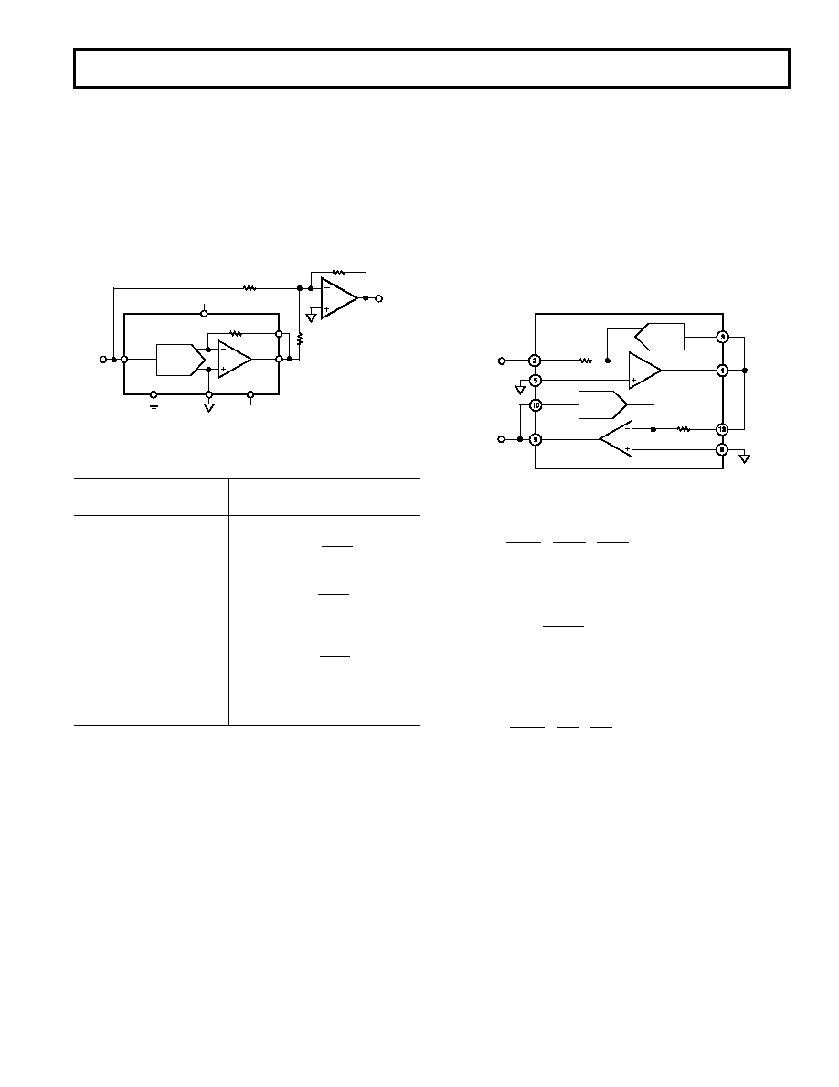
PROGRAMMABLE GAIN AMPLIFIER (PGA)
The dual DAC/amplifier combination along with access to RFB
make the AD7837 ideal as a programmable gain amplifier. In this
application, the DAC functions as a programmable resistor in the
amplifier feedback loop. This type of configuration is shown
in Figure 17 and is suitable for ac gain control. The circuit con-
sists of two PGAs in series. Use of a dual configuration provides
greater accuracy over a wider dynamic range than a single PGA
solution. The overall system gain is the product of the individual
gain stages. The effective gains for each stage are controlled by
the DAC codes. As the code decreases, the effective DAC
resistance increases, and so the gain also increases.
DAC B
AGNDA
VOUTB
VREFB
VIN
RFBB
AD7837
VOUT
RFBA
AGNDB
DAC A
VOUTA
VREFA
Figure 17. Dual PGA Circuit
The transfer function is given by
VOUT
VIN
=
REQA
RFBA
×
REQB
RFBB
(1)
where REQA, REQB are the effective DAC resistances controlled
by the digital input code:
REQ
=
212 RIN
N
(2)
where RIN is the DAC input resistance and is equal to RFB and
N = DAC input code in decimal.
The transfer function in (1) thus simplifies to
VOUT
VIN
=
212
N A
×
212
NB
(3)
where NA = DAC A input code in decimal and NB = DAC B
input code in decimal.
NA, NB may be programmed between 1 and (2
12–1). The zero
code is not allowed as it results in an open loop amplifier
response. To minimize errors, the digital codes NA and NB
should be chosen to be equal to or as close as possible to each
other to achieve the required gain.
BIPOLAR OPERATION
(4-QUADRANT MULTIPLICATION)
Figure 16 shows the AD7837/AD7847 connected for bipolar
operation. The coding is offset binary as shown in Table IV.
When VIN is an ac signal, the circuit performs 4-quadrant multi-
plication. To maintain the gain error specifications, resistors R1,
R2 and R3 should be ratio matched to 0.01%. Note that on the
AD7847 the feedback resistor RFB is internally connected to
VOUT.
DAC A
AGNDA
VOUTA
VREFA
VIN
DGND
VSS
RFBA
*
VDD
AD7837
AD7847
*INTERNALLY
CONNECTED
ON AD7847
R3
10k
R1
20k
AD711
R2
20k
VOUT
VSS
Figure 16. Bipolar Offset Binary Operation
Table IV. Bipolar Code Table
DAC Latch Contents
MSB
LSB
Analog Output, VOUT
1111 1111 1111
+V
IN
×
2047
2048
1000 0000 0001
+V
IN
×
1
2048
1000 0000 0000
0 V
0111 1111 1111
–VIN
×
1
2048
0000 0000 0000
–VIN
×
2048
= –V
IN
Note 1 LSB =
V
IN
2048
.
相关PDF资料 |
PDF描述 |
|---|---|
| AD660ANZ | IC DAC 16BIT MONO W/VREF 24-DIP |
| AD766ANZ | IC DAC 16BIT W/REF DSP 16-DIP |
| VE-BWL-MY-F1 | CONVERTER MOD DC/DC 28V 50W |
| AD7228ACPZ | IC DAC 8BIT OCTAL W/AMP 28-PLCC |
| VE-BWK-MY-F1 | CONVERTER MOD DC/DC 40V 50W |
相关代理商/技术参数 |
参数描述 |
|---|---|
| AD7847BRZ | 制造商:Analog Devices 功能描述:IC 12-BIT DAC |
| AD7847BRZ-REEL | 功能描述:IC DAC 12BIT DUAL MULT 24-SOIC RoHS:是 类别:集成电路 (IC) >> 数据采集 - 数模转换器 系列:- 产品培训模块:Data Converter Fundamentals DAC Architectures 标准包装:750 系列:- 设置时间:7µs 位数:16 数据接口:并联 转换器数目:1 电压电源:双 ± 功率耗散(最大):100mW 工作温度:0°C ~ 70°C 安装类型:表面贴装 封装/外壳:28-LCC(J 形引线) 供应商设备封装:28-PLCC(11.51x11.51) 包装:带卷 (TR) 输出数目和类型:1 电压,单极;1 电压,双极 采样率(每秒):143k |
| AD7847SQ | 制造商:Rochester Electronics LLC 功能描述:LC2MOS COMPLETE, DUAL 12-BIT MDAC, PARALLEL LOADING STRUCTUR - Bulk 制造商:Analog Devices 功能描述: |
| AD7847SQ/883B | 制造商:AD 制造商全称:Analog Devices 功能描述:LC2MOS Complete, Dual 12-Bit MDACs |
| AD7847SQ883B | 制造商:AD 制造商全称:Analog Devices 功能描述:LC2MOS Complete, Dual 12-Bit MDACs |
发布紧急采购,3分钟左右您将得到回复。