参数资料
| 型号: | AD7849CR-REEL |
| 厂商: | Analog Devices Inc |
| 文件页数: | 18/20页 |
| 文件大小: | 0K |
| 描述: | IC DAC 16BIT SRL INP 20-SOIC |
| 产品培训模块: | Data Converter Fundamentals DAC Architectures |
| 标准包装: | 1,000 |
| 设置时间: | 7µs |
| 位数: | 16 |
| 数据接口: | 串行 |
| 转换器数目: | 1 |
| 电压电源: | 模拟和数字,双 ± |
| 功率耗散(最大): | 100mW |
| 工作温度: | -40°C ~ 85°C |
| 安装类型: | 表面贴装 |
| 封装/外壳: | 20-SOIC(0.295",7.50mm 宽) |
| 供应商设备封装: | 20-SOIC W |
| 包装: | 带卷 (TR) |
| 输出数目和类型: | 1 电压,单极;1 电压,双极 |
| 采样率(每秒): | 143k |
AD7849
Rev. C | Page 7 of 20
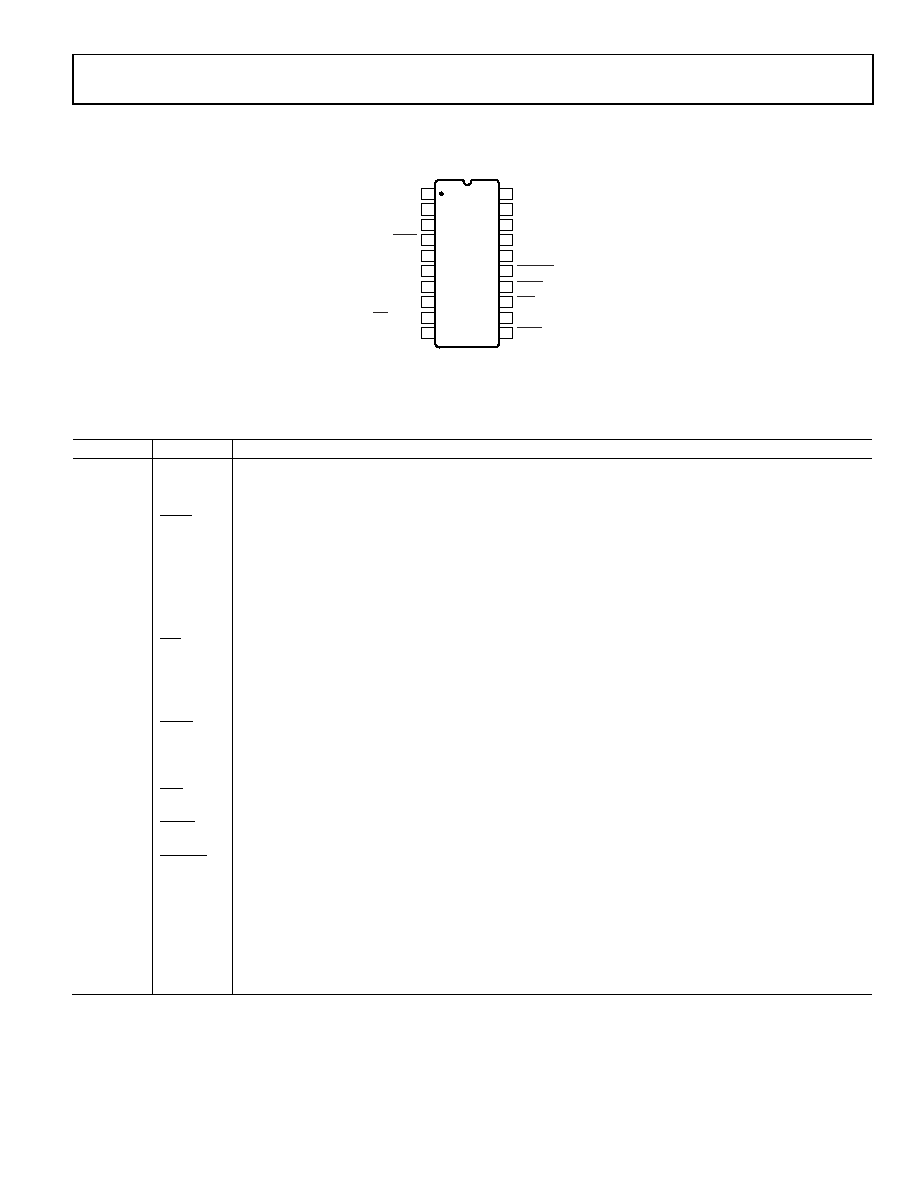
PIN CONFIGURATION AND FUNCTION DESCRIPTIONS
VREF+
VDD
NC
VOUT
ROFS
VREF–
VSS
SYNC
RSTIN
RSTOUT
AGND
SCLK
VCC
SDOUT
DCEN
BIN/COMP
DGND
LDAC
SDIN
CLR
1
2
3
4
20
19
18
17
5
16
6
15
7
14
8
13
9
12
10
11
NC = NO CONNECT. DO NOT CONNECT TO THIS PIN.
AD7849
TOP VIEW
(Not to Scale)
010
08-
003
Figure 2. Pin Configuration
Table 6. Pin Function Descriptions
Pin No.
Mnemonic
Description
1
VREF+
VREF+ Input. The DAC is specified for VREF+ of 5 V. The DAC is fully multiplying so that the VREF+ range is +5 V to –5 V.
2
VREF
VREF Input. The DAC is specified for VREF of –5 V. The DAC is fully multiplying so that the VREF range is –5 V to +5 V.
3
VSS
Negative supply for the analog circuitry. This is nominally –15 V.
4
SYNC
Data Synchronization Logic Input. When it goes low, the internal logic is initialized in readiness for a new data-word.
5
SCLK
Serial Clock Logic Input. Data is clocked into the input register on each SCLK falling edge.
6
VCC
Positive supply for the digital circuitry. This is nominally 5 V.
7
SDOUT
Serial Data Output. With DCEN at Logic 1, this output is enabled, and the serial data in the input shift register is
clocked out on each rising edge of SCLK.
8
DCEN
Daisy-Chain Enable Logic Input. Connect this pin high if a daisy-chain interface is being used; otherwise, this
pin must be connected low.
9
BIN/COMP
Logic Input. This input selects the data format to be either binary or twos complement. In the unipolar output
range, natural binary format is selected by connecting the input to Logic 0. In the bipolar output range, offset
binary is selected by connecting this input to Logic 0, and twos complement is selected by connecting it to a
Logic 1.
10
DGND
Digital Ground. Ground reference point for the on-chip digital circuitry.
11
LDAC
Load DAC Logic Input. This input updates the DAC output. The DAC output is updated on the falling edge of
this signal, or alternatively, if this input is permanently low, an automatic update mode is selected where the
DAC is updated on the 16th falling SCLK edge.
12
SDIN
Serial Data Input. The 16-bit serial data-word is applied to this input.
13
CLR
Clear Logic Input. Taking this input low sets VOUT to 0 V in both the unipolar output range and the bipolar twos
complement output range. It sets VOUT to VREF– in the offset binary bipolar output range.
14
RSTIN
Reset Logic Input. This input allows external access to the internal reset logic. Applying Logic 0 to this input,
resets the DAC output to 0 V. In normal operation, it should be tied to Logic 1.
15
RSTOUT
Reset Logic Output. This is the output from the on-chip voltage monitor used in the reset circuit. It can be used
to control other system components, if desired.
16
AGND
This is the analog ground for the device. It is the point to which the output gets shorted in reset mode.
17
VDD
Positive Supply for the Analog Circuitry. This is 15 V nominal.
18
NC
No Connect. Leave unconnected.
19
VOUT
DAC Output Voltage Pin.
20
ROFS
Input to Summing Resistor of DAC Output Amplifier. This is used to select the output voltage ranges. Also, see
相关PDF资料 |
PDF描述 |
|---|---|
| AD7564AR-B | IC DAC 12BIT QUAD 3.3V LP 28SOIC |
| VI-B63-MU | CONVERTER MOD DC/DC 24V 200W |
| AD7564BR | IC DAC 12BIT LC2MOS QUAD 28-SOIC |
| VE-23X-IV-F2 | CONVERTER MOD DC/DC 5.2V 150W |
| VE-B6P-MU | CONVERTER MOD DC/DC 13.8V 200W |
相关代理商/技术参数 |
参数描述 |
|---|---|
| AD7849CRZ | 功能描述:IC DAC 14/16BIT SRL-IN 20-SOIC RoHS:是 类别:集成电路 (IC) >> 数据采集 - 数模转换器 系列:- 标准包装:1 系列:- 设置时间:4.5µs 位数:12 数据接口:串行,SPI? 转换器数目:1 电压电源:单电源 功率耗散(最大):- 工作温度:-40°C ~ 125°C 安装类型:表面贴装 封装/外壳:8-SOIC(0.154",3.90mm 宽) 供应商设备封装:8-SOICN 包装:剪切带 (CT) 输出数目和类型:1 电压,单极;1 电压,双极 采样率(每秒):* 其它名称:MCP4921T-E/SNCTMCP4921T-E/SNRCTMCP4921T-E/SNRCT-ND |
| AD7849CRZ-REEL | 功能描述:IC DAC 14/16BIT SRL-IN 20-SOIC RoHS:是 类别:集成电路 (IC) >> 数据采集 - 数模转换器 系列:- 产品培训模块:Data Converter Fundamentals DAC Architectures 标准包装:750 系列:- 设置时间:7µs 位数:16 数据接口:并联 转换器数目:1 电压电源:双 ± 功率耗散(最大):100mW 工作温度:0°C ~ 70°C 安装类型:表面贴装 封装/外壳:28-LCC(J 形引线) 供应商设备封装:28-PLCC(11.51x11.51) 包装:带卷 (TR) 输出数目和类型:1 电压,单极;1 电压,双极 采样率(每秒):143k |
| AD7849TQ | 制造商:AD 制造商全称:Analog Devices 功能描述:Serial Input, 14-Bit/16-Bit DAC |
| AD784ARQZREEL | 制造商:ANALOG 功能描述:NEW |
| AD7850JP | 制造商:Rochester Electronics LLC 功能描述:- Bulk |
发布紧急采购,3分钟左右您将得到回复。