参数资料
| 型号: | AD7849CR-REEL |
| 厂商: | Analog Devices Inc |
| 文件页数: | 3/20页 |
| 文件大小: | 0K |
| 描述: | IC DAC 16BIT SRL INP 20-SOIC |
| 产品培训模块: | Data Converter Fundamentals DAC Architectures |
| 标准包装: | 1,000 |
| 设置时间: | 7µs |
| 位数: | 16 |
| 数据接口: | 串行 |
| 转换器数目: | 1 |
| 电压电源: | 模拟和数字,双 ± |
| 功率耗散(最大): | 100mW |
| 工作温度: | -40°C ~ 85°C |
| 安装类型: | 表面贴装 |
| 封装/外壳: | 20-SOIC(0.295",7.50mm 宽) |
| 供应商设备封装: | 20-SOIC W |
| 包装: | 带卷 (TR) |
| 输出数目和类型: | 1 电压,单极;1 电压,双极 |
| 采样率(每秒): | 143k |
AD7849
Rev. C | Page 11 of 20
CIRCUIT DESCRIPTION
DIGITAL-TO-ANALOG CONVERSION
are three on-chip DACs, each of which has its own buffer amplifier.
DAC1 and DAC2 are 4-bit DACs. They share a 16-resistor string,
but they have their own analog multiplexers. The voltage reference
is applied to the resistor string. DAC3 is a 12-bit voltage mode
DAC with its own output stage.
The four MSBs of the 16-bit digital input code drive DAC1 and
DAC2, while the 12 LSBs control DAC3. Using DAC1 and DAC2,
the MSBs select a pair of adjacent nodes on the resistor string
and present that voltage to the positive and negative inputs of
DAC3. This DAC interpolates between these two voltages to
produce the analog output voltage.
To prevent nonmonotonicity in the DAC due to amplifier offset
voltages, DAC1 and DAC2 leap-frog along the resistor string.
For example, when switching from Segment 1 to Segment 2, DAC1
switches from the bottom of Segment 1 to the top of Segment 2
while DAC 2 remains connected to the top of Segment 1. The
code driving DAC3 is automatically complemented to compensate
for the inversion of its inputs. This means that any linearity
effects due to amplifier offset voltages remain unchanged when
switching from one segment to the next, and 16-bit monotonicity is
ensured if DAC3 is monotonic. Therefore, 12-bit resistor matching
in DAC3 guarantees overall 16-bit monotonicity. This is much
more achievable than the 16-bit matching that a conventional
R-2R structure would need.
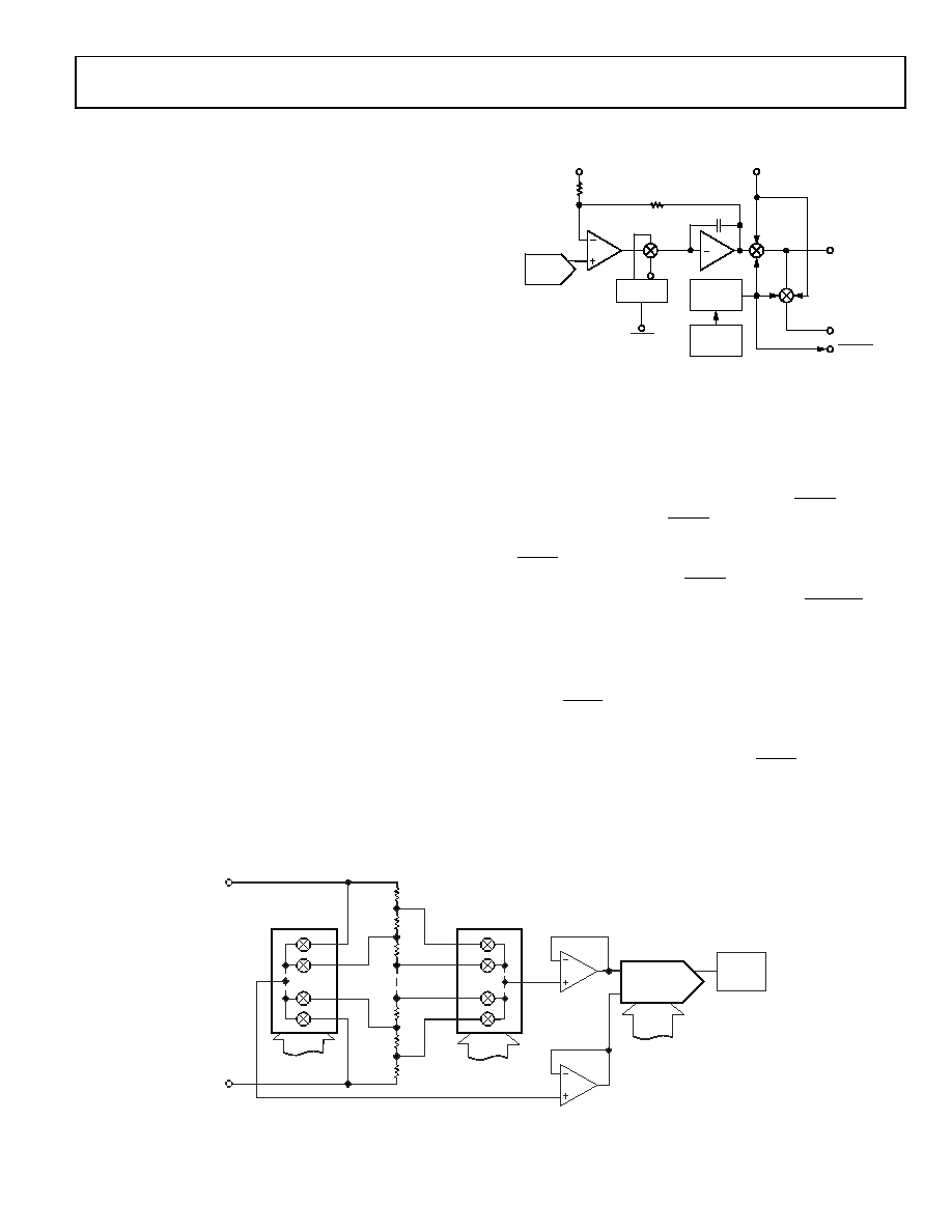
Output Stage
of driving a 2 kΩ load in parallel with 200 pF. The feedback and
offset resistors allow the output stage to be configured for gains of
1 or 2. Additionally, the offset resistor can be used to shift the
output range. The AD7849 has a special feature to ensure output
stability during power-up and power-down sequences. This feature
is available for control applications where actuators must not be
allowed to move in an uncontrolled fashion.
LOGIC
CIRCUITRY
ONE-SHOT
LDAC
DAC 3
G3
C1
R
10k
R
10k
ROFS
RSTIN
G1
VOUT
AGND
RSTOUT
G2
VOLTAGE
MONITOR
01008
-015
Figure 14. Output Stage
When the supply voltages are changing, the VOUT pin is clamped
to 0 V via a low impedance path. To prevent the output of A3
from being shorted to 0 V during this time, Transmission Gate G1
is opened. These conditions are maintained until the power
supplies stabilize, and a valid word is written to the DAC register.
At this time, G2 opens and G1 closes. Both transmission gates
are also externally controllable via the reset in (RSTIN) control
input. For instance, if the RSTIN input is driven from a battery
supervisor chip, then at power-off or during a brownout, the
RSTIN input will be driven low to open G1 and closeG2. The
DAC has to be reloaded, with RSTIN high, to reenable the output.
Conversely, the on-chip voltage detector output (RSTOUT) is
also available to the user to control other parts of the system.
The AD7849 output buffer is configured as a track-and-hold
amplifier. Although normally tracking its input, this amplifier
isplaced in hold mode for approximately 5 μs after the leading
edge of LDAC. This short state keeps the DAC output at its
previous voltage while the
is internally changing to its
new value. therefore, any glitches that occur in the transition are
not seen at the output. In systems where
LDAC is permanently
low, deglitching is not in operation.
10/12
DAC 2
A1
A2
DAC 3
10-BIT/12-BIT
DAC
S2
S4
S14
S16
DB15 TO DB12
DAC 1
S1
S3
S15
S17
VREF+
VREF–
OUTPUT
STAGE
R
01
008-016
Figure 15. Digital-to-Analog Conversion
相关PDF资料 |
PDF描述 |
|---|---|
| AD7564AR-B | IC DAC 12BIT QUAD 3.3V LP 28SOIC |
| VI-B63-MU | CONVERTER MOD DC/DC 24V 200W |
| AD7564BR | IC DAC 12BIT LC2MOS QUAD 28-SOIC |
| VE-23X-IV-F2 | CONVERTER MOD DC/DC 5.2V 150W |
| VE-B6P-MU | CONVERTER MOD DC/DC 13.8V 200W |
相关代理商/技术参数 |
参数描述 |
|---|---|
| AD7849CRZ | 功能描述:IC DAC 14/16BIT SRL-IN 20-SOIC RoHS:是 类别:集成电路 (IC) >> 数据采集 - 数模转换器 系列:- 标准包装:1 系列:- 设置时间:4.5µs 位数:12 数据接口:串行,SPI? 转换器数目:1 电压电源:单电源 功率耗散(最大):- 工作温度:-40°C ~ 125°C 安装类型:表面贴装 封装/外壳:8-SOIC(0.154",3.90mm 宽) 供应商设备封装:8-SOICN 包装:剪切带 (CT) 输出数目和类型:1 电压,单极;1 电压,双极 采样率(每秒):* 其它名称:MCP4921T-E/SNCTMCP4921T-E/SNRCTMCP4921T-E/SNRCT-ND |
| AD7849CRZ-REEL | 功能描述:IC DAC 14/16BIT SRL-IN 20-SOIC RoHS:是 类别:集成电路 (IC) >> 数据采集 - 数模转换器 系列:- 产品培训模块:Data Converter Fundamentals DAC Architectures 标准包装:750 系列:- 设置时间:7µs 位数:16 数据接口:并联 转换器数目:1 电压电源:双 ± 功率耗散(最大):100mW 工作温度:0°C ~ 70°C 安装类型:表面贴装 封装/外壳:28-LCC(J 形引线) 供应商设备封装:28-PLCC(11.51x11.51) 包装:带卷 (TR) 输出数目和类型:1 电压,单极;1 电压,双极 采样率(每秒):143k |
| AD7849TQ | 制造商:AD 制造商全称:Analog Devices 功能描述:Serial Input, 14-Bit/16-Bit DAC |
| AD784ARQZREEL | 制造商:ANALOG 功能描述:NEW |
| AD7850JP | 制造商:Rochester Electronics LLC 功能描述:- Bulk |
发布紧急采购,3分钟左右您将得到回复。