- 您现在的位置:买卖IC网 > PDF目录10184 > AD7854AR (Analog Devices Inc)IC ADC 12BIT PARALLEL LP 28-SOIC PDF资料下载
参数资料
| 型号: | AD7854AR |
| 厂商: | Analog Devices Inc |
| 文件页数: | 5/28页 |
| 文件大小: | 0K |
| 描述: | IC ADC 12BIT PARALLEL LP 28-SOIC |
| 标准包装: | 27 |
| 位数: | 12 |
| 采样率(每秒): | 200k |
| 数据接口: | 并联 |
| 转换器数目: | 2 |
| 功率耗散(最大): | 30mW |
| 电压电源: | 模拟和数字 |
| 工作温度: | -40°C ~ 85°C |
| 安装类型: | 表面贴装 |
| 封装/外壳: | 28-SOIC(0.295",7.50mm 宽) |
| 供应商设备封装: | 28-SOIC W |
| 包装: | 管件 |
| 输入数目和类型: | 1 个伪差分,单极;1 个伪差分,双极 |
第1页第2页第3页第4页当前第5页第6页第7页第8页第9页第10页第11页第12页第13页第14页第15页第16页第17页第18页第19页第20页第21页第22页第23页第24页第25页第26页第27页第28页
AD7854/AD7854L
REV. B
–13–
When using the software conversion start for maximum
throughput, the user must ensure the control register write
operation extends beyond the falling edge of BUSY. The falling
edge of BUSY resets the
CONVST bit to 0 and allows it to be
reprogrammed to 1 to start the next conversion.
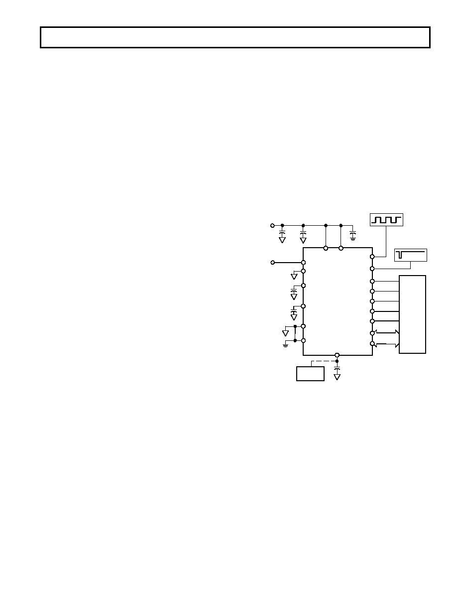
TYPICAL CONNECTION DIAGRAM
Figure 8 shows a typical connection diagram for the AD7854/
AD7854L. The AGND and the DGND pins are connected
together at the device for good noise suppression. The first
CONVST applied after power-up starts a self-calibration
sequence. This is explained in the calibration section of the data
sheet. Applying the
RD and CS signals causes the conversion
result to be output on the 12 data pins. Note that after power is
applied to AVDD and DVDD, and the CONVST signal is applied,
the part requires (70 ms + 1/sample rate) for the internal refer-
ence to settle and for the self-calibration to be completed.
4MHz/1.8MHz
OSCILLATOR
AVDD DVDD
AIN(+)
AIN(–)
CREF1
CREF2
DB11
DB0
CONVST
AGND
DGND
CLKIN
REFIN /REFOUT
AD7854/
AD7854L
ANALOG
SUPPLY
+3V TO +5V
0.1 F
10 F
0.1 F
0.01 F
CONVERSION
START SIGNAL
0.1nF EXTERNAL REFERENCE
0.1 F ON-CHIP REFERENCE
0V TO 2.5V
INPUT
OPTIONAL
EXTERNAL
REFERENCE
CS
RD
WR
BUSY
AD780/
REF192
C/ P
HBEN
Figure 8. Typical Circuit
For applications where power consumption is a major concern,
the power-down options can be programmed by writing to the
part. See Power-Down section for more detail on low power
applications.
CIRCUIT INFORMATION
The AD7854/AD7854L is a fast, 12-bit single supply A/D con-
verter. The part requires an external 4 MHz/1.8 MHz master
clock (CLKIN), two CREF capacitors, a CONVST signal to start
conversion and power supply decoupling capacitors. The part
provides the user with track/hold, on-chip reference, calibration
features, A/D converter and parallel interface logic functions on
a single chip. The A/D converter section of the AD7854/
AD7854L consists of a conventional successive-approximation
converter based around a capacitor DAC. The AD7854/
AD7854L accepts an analog input range of 0 to +VREF. VREF
can be tied to VDD. The reference input to the part connected
via a 150 k
resistor to the internal 2.5 V reference and to the
on-chip buffer.
A major advantage of the AD7854/AD7854L is that a conver-
sion can be initiated in software as well as applying a signal to
the
CONVST pin. The part is available in a 28-Lead SSOP
package, and this offers the user considerable space saving advan-
tages over alternative solutions. The AD7854L version typically
consumes only 5.5 mW making it ideal for battery-powered
applications.
CONVERTER DETAILS
The master clock for the part is applied to the CLKIN pin.
Conversion is initiated on the AD7854/AD7854L by pulsing the
CONVST input or by writing to the control register and setting
the CONVST bit to 1. On the rising edge of
CONVST (or at the
end of the control register write operation), the on-chip track/
hold goes from track to hold mode. The falling edge of the CLKIN
signal which follows the rising edge of
CONVST initates the
conversion, provided the rising edge of
CONVST (or WR when
converting via the control register) occurs typically at least 10 ns
before this CLKIN edge. The conversion takes 16.5 CLKIN
periods from this CLKIN falling edge. If the 10 ns setup time is
not met, the conversion takes 17.5 CLKIN periods.
The time required by the AD7854/AD7854L to acquire a signal
depends upon the source resistance connected to the AIN(+)
input. Please refer to the Acquisition Time section for more
details.
When a conversion is completed, the BUSY output goes low,
and the result of the conversion can be read by accessing the
data through the data bus. To obtain optimum performance
from the part, read or write operations should not occur during
the conversion or less than 200 ns prior to the next
CONVST
rising edge. Reading/writing during conversion typically de-
grades the Signal to (Noise + Distortion) by less than 0.5 dBs.
The AD7854 can operate at throughput rates of over 200 kSPS
(up to 100 kSPS for the AD7854L).
With the AD7854L, 100 kSPS throughput can be obtained as
follows: the CLKIN and
CONVST signals are arranged to give
a conversion time of 16.5 CLKIN periods as described above
and 1.5 CLKIN periods are allowed for the acquisition time.
With a 1.8 MHz clock, this gives a full cycle time of 10
s,
which equates to a throughput rate of 100 kSPS.
相关PDF资料 |
PDF描述 |
|---|---|
| ADM3312EARUZ-REEL | IC TXRX RS-232 3:3 2.7V 24TSSOP |
| VE-25K-IU-F3 | CONVERTER MOD DC/DC 40V 200W |
| VI-2NH-CU-F3 | CONVERTER MOD DC/DC 52V 200W |
| VI-263-IW-S | CONVERTER MOD DC/DC 24V 100W |
| MS27468T15F18SB | CONN RCPT 18POS JAM NUT W/SCKT |
相关代理商/技术参数 |
参数描述 |
|---|---|
| AD7854AR-REEL | 制造商:Analog Devices 功能描述:ADC Single SAR 200ksps 12-bit Parallel 28-Pin SOIC W T/R 制造商:Analog Devices 功能描述:ADC SGL SAR 200KSPS 12-BIT PARALLEL 28SOIC W - Tape and Reel |
| AD7854ARS | 功能描述:IC ADC 12BIT PARALLEL LP 28-SSOP RoHS:否 类别:集成电路 (IC) >> 数据采集 - 模数转换器 系列:- 标准包装:1,000 系列:- 位数:12 采样率(每秒):300k 数据接口:并联 转换器数目:1 功率耗散(最大):75mW 电压电源:单电源 工作温度:0°C ~ 70°C 安装类型:表面贴装 封装/外壳:24-SOIC(0.295",7.50mm 宽) 供应商设备封装:24-SOIC 包装:带卷 (TR) 输入数目和类型:1 个单端,单极;1 个单端,双极 |
| AD7854ARS-REEL | 功能描述:IC ADC 12BIT PARALLEL LP 28-SSOP RoHS:否 类别:集成电路 (IC) >> 数据采集 - 模数转换器 系列:- 标准包装:1,000 系列:- 位数:12 采样率(每秒):300k 数据接口:并联 转换器数目:1 功率耗散(最大):75mW 电压电源:单电源 工作温度:0°C ~ 70°C 安装类型:表面贴装 封装/外壳:24-SOIC(0.295",7.50mm 宽) 供应商设备封装:24-SOIC 包装:带卷 (TR) 输入数目和类型:1 个单端,单极;1 个单端,双极 |
| AD7854ARSZ | 功能描述:IC ADC 12BIT PARALLEL LP 28-SSOP RoHS:是 类别:集成电路 (IC) >> 数据采集 - 模数转换器 系列:- 其它有关文件:TSA1204 View All Specifications 标准包装:1 系列:- 位数:12 采样率(每秒):20M 数据接口:并联 转换器数目:2 功率耗散(最大):155mW 电压电源:模拟和数字 工作温度:-40°C ~ 85°C 安装类型:表面贴装 封装/外壳:48-TQFP 供应商设备封装:48-TQFP(7x7) 包装:Digi-Reel® 输入数目和类型:4 个单端,单极;2 个差分,单极 产品目录页面:1156 (CN2011-ZH PDF) 其它名称:497-5435-6 |
| AD7854ARZ | 功能描述:IC ADC 12BIT PARALLEL LP 28SOIC RoHS:是 类别:集成电路 (IC) >> 数据采集 - 模数转换器 系列:- 标准包装:1,000 系列:- 位数:12 采样率(每秒):300k 数据接口:并联 转换器数目:1 功率耗散(最大):75mW 电压电源:单电源 工作温度:0°C ~ 70°C 安装类型:表面贴装 封装/外壳:24-SOIC(0.295",7.50mm 宽) 供应商设备封装:24-SOIC 包装:带卷 (TR) 输入数目和类型:1 个单端,单极;1 个单端,双极 |
发布紧急采购,3分钟左右您将得到回复。