- 您现在的位置:买卖IC网 > PDF目录10191 > AD7858BRZ-REEL (Analog Devices Inc)IC ADC 12BIT 8CHAN SRL 24SOIC PDF资料下载
参数资料
| 型号: | AD7858BRZ-REEL |
| 厂商: | Analog Devices Inc |
| 文件页数: | 13/32页 |
| 文件大小: | 0K |
| 描述: | IC ADC 12BIT 8CHAN SRL 24SOIC |
| 标准包装: | 1,000 |
| 位数: | 12 |
| 采样率(每秒): | 200k |
| 数据接口: | 8051,QSPI?,串行,SPI? µP |
| 转换器数目: | 2 |
| 功率耗散(最大): | 33mW |
| 电压电源: | 模拟和数字 |
| 工作温度: | -40°C ~ 85°C |
| 安装类型: | 表面贴装 |
| 封装/外壳: | 24-SOIC(0.295",7.50mm 宽) |
| 供应商设备封装: | 24-SOIC W |
| 包装: | 带卷 (TR) |
| 输入数目和类型: | 8 个单端,单极;4 个伪差分,单极 |
第1页第2页第3页第4页第5页第6页第7页第8页第9页第10页第11页第12页当前第13页第14页第15页第16页第17页第18页第19页第20页第21页第22页第23页第24页第25页第26页第27页第28页第29页第30页第31页第32页
REV. B
–20–
AD7858/AD7858L
The recommended value of the external capacitor is 100 nF;
this gives a power-up time of approximately 135 ms before a
calibration is initiated and normal operation should commence.
When CREF is fully charged, the power-up time from a hardware
or software power-down reduces to 5
s. This is because an
internal switch opens to provide a high impedance discharge
path for the reference capacitor during power-down—see Figure
23. An added advantage of the low charge leakage from the
reference capacitor during power-down is that even though the
reference is being powered down between conversions, the
reference capacitor holds the reference voltage to within
0.5 LSBs with throughput rates of 100 samples/second and
over with a full power-down between conversions. A high input
impedance op amp like the AD707 should be used to buffer this
reference capacitor if it is being used externally. Note, if the
AD7858 is left in its power-down state for more than 100 ms,
the charge on CREF will start to leak away and the power-up
time will increase. If this long power-up time is a problem, the
user can use a partial power-down for the last conversion so the
reference remains powered up.
AD7858
REFIN/REFOUT
EXTERNAL
CAPACITOR
SWITCH OPENS
DURING POWER-DOWN
BUF
ON-CHIP
REFERENCE
TO OTHER
CIRCUITRY
Figure 23. On-Chip Reference During Power-Down
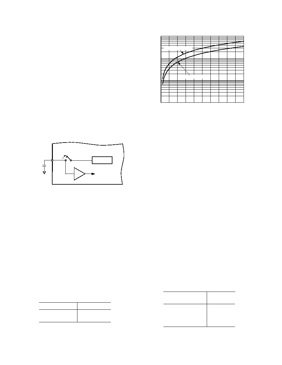
POWER VS. THROUGHPUT RATE
The main advantage of a full power-down after a conversion is
that it significantly reduces the power consumption of the part
at lower throughput rates. When using this mode of operation,
the AD7858 is only powered up for the duration of the conver-
sion. If the power-up time of the AD7858 is taken to be 5
s
and it is assumed that the current during power-up is 4 mA typ,
then power consumption as a function of throughput can easily
be calculated. The AD7858 has a conversion time of 4.6
s
with a 4 MHz external clock. This means the AD7858 con-
sumes 4 mA typ, (or 12 mW typ VDD = 3 V) for 9.6
s in every
conversion cycle if the device is powered down at the end of a
conversion. If the throughput rate is 1 kSPS, the cycle time is
1000
s and the average power dissipated during each cycle is
(9.6/1000)
× (12 mW) = 115 W. The graph, Figure 24, shows
the power consumption of the AD7858 as a function of through-
put. Table VII lists the power consumption for various through-
put rates.
Table VII. Power Consumption vs. Throughput
Throughput Rate
Power
1 kSPS
115
W
10 kSPS
1.15 mW
POWER
–
mW
0.01
1
10
THROUGHPUT – kSPS
0
10
20
30
40
50
0.1
515
25
35
45
AD7858 (4MHz CLK)
AD7858L (1.8MHz CLK)
Figure 24. Power vs. Throughput Rate
CALIBRATION SECTION
Calibration Overview
The automatic calibration that is performed on power-up en-
sures that the calibration options covered in this section will not
be required in a significant amount of applications. The user
will not have to initiate a calibration unless the operating condi-
tions change (CLKIN frequency, analog input mode, reference
voltage, temperature, and supply voltages). The AD7858/
AD7858L have a number of calibration features that may be
required in some applications and there are a number of advan-
tages in performing these different types of calibration. First,
the internal errors in the ADC can be reduced significantly to
give superior dc performance, and secondly, system offset and
gain errors can be removed. This allows the user to remove
reference errors (whether it be internal or external reference)
and to make use of the full dynamic range of the AD7858/
AD7858L by adjusting the analog input range of the part for a
specific system.
There are two main calibration modes on the AD7858/AD7858L,
self-calibration and system calibration. There are various op-
tions in both self-calibration and system calibration as outlined
previously in Table IV. All the calibration functions can be
initiated by pulsing the
CAL pin or by writing to the control
register and setting the STCAL bit to one. The timing diagrams
that follow involve using the
CAL pin.
The duration of each of the different types of calibrations is
given in Table VIII for the AD7858 with a 4 MHz master clock.
These calibration times are master clock dependent. Therefore,
the calibrating times for the AD7858L (CLKIN = 1.8 MHz)
will be longer than those quoted in Table VIII.
Table VIII. Calibration Times (AD7858 with 4 MHz CLKIN)
Type of Self- or
System Calibration
Time
Full
31.25 ms
Offset + Gain
6.94 ms
Offset
3.47 ms
Gain
3.47 ms
相关PDF资料 |
PDF描述 |
|---|---|
| ADM3202ARU-REEL | IC TXRX DUAL RS-232 3.3V 16TSSOP |
| ADM3222ARU-REEL | IC TXRX RS232 3.3V W/SD 20TSSOP |
| MS27467E11F4SA | CONN PLUG 4POS STRAIGHT W/SCKT |
| MS27466P17A35SA | CONN RCPT 55POS WALL MNT W/SCKT |
| MS3106E28-12P | CONN PLUG 26POS STRAIGHT W/PINS |
相关代理商/技术参数 |
参数描述 |
|---|---|
| AD7858L | 制造商:AD 制造商全称:Analog Devices 功能描述:3 V to 5 V Single Supply, 200 kSPS 8-Channel, 12-Bit Sampling ADC |
| AD7858LAN | 制造商:Analog Devices 功能描述: |
| AD7858LAN3 | 制造商:AD 制造商全称:Analog Devices 功能描述:3 V to 5 V Single Supply, 200 kSPS 8-Channel, 12-Bit Sampling ADC |
| AD7858LANZ | 功能描述:IC ADC 12BIT 8CHAN SRL 24DIP RoHS:是 类别:集成电路 (IC) >> 数据采集 - 模数转换器 系列:- 标准包装:1,000 系列:- 位数:12 采样率(每秒):300k 数据接口:并联 转换器数目:1 功率耗散(最大):75mW 电压电源:单电源 工作温度:0°C ~ 70°C 安装类型:表面贴装 封装/外壳:24-SOIC(0.295",7.50mm 宽) 供应商设备封装:24-SOIC 包装:带卷 (TR) 输入数目和类型:1 个单端,单极;1 个单端,双极 |
发布紧急采购,3分钟左右您将得到回复。