- 您现在的位置:买卖IC网 > PDF目录10191 > AD7858BRZ-REEL (Analog Devices Inc)IC ADC 12BIT 8CHAN SRL 24SOIC PDF资料下载
参数资料
| 型号: | AD7858BRZ-REEL |
| 厂商: | Analog Devices Inc |
| 文件页数: | 21/32页 |
| 文件大小: | 0K |
| 描述: | IC ADC 12BIT 8CHAN SRL 24SOIC |
| 标准包装: | 1,000 |
| 位数: | 12 |
| 采样率(每秒): | 200k |
| 数据接口: | 8051,QSPI?,串行,SPI? µP |
| 转换器数目: | 2 |
| 功率耗散(最大): | 33mW |
| 电压电源: | 模拟和数字 |
| 工作温度: | -40°C ~ 85°C |
| 安装类型: | 表面贴装 |
| 封装/外壳: | 24-SOIC(0.295",7.50mm 宽) |
| 供应商设备封装: | 24-SOIC W |
| 包装: | 带卷 (TR) |
| 输入数目和类型: | 8 个单端,单极;4 个伪差分,单极 |
第1页第2页第3页第4页第5页第6页第7页第8页第9页第10页第11页第12页第13页第14页第15页第16页第17页第18页第19页第20页当前第21页第22页第23页第24页第25页第26页第27页第28页第29页第30页第31页第32页
REV. B
–28–
AD7858/AD7858L
MICROPROCESSOR INTERFACING
In many applications, the user may not require the facility of
writing to most of the on-chip registers. The only writing neces-
sary is to set the input channel configuration. After this the
CONVST is applied, a conversion is performed, and the result
may be read using the SCLK to clock out the data from the
output register on to the DOUT pin. At the same time a write
operation occurs and this may consist of all 0s where no data is
written to the part or may set a different input channel configu-
ration for the next conversion. The SCLK may be connected to
the CLKIN pin if the user does not want to have to provide
separate serial and master clocks. With this arrangement the
SYNC signal must be low for 16 SCLK cycles for the read and
write operations.
DIN
DOUT
SYNC
CONVST
CLKIN
SCLK
AD7858/
AD7858L
4MHz/1.8MHz
MASTER CLOCK
SYNC SIGNAL TO
GATE THE SCLK
SERIAL DATA
OUTPUT
CONVERSION START
SERIAL DATA INPUT
Figure 36. Simplified Interface Diagram
AD7858/AD7858L to 8XC51 Interface
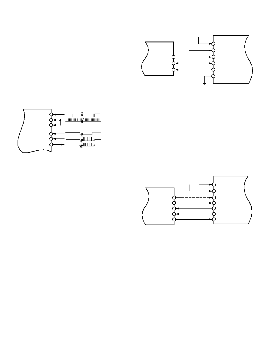
Figure 37 shows the AD7858/AD7858L interface to the
8XC51. The 8XL51 is for interfacing to the AD7858/AD7858L
when the supply is at 3 V. The 8XC51 only runs at 5 V. The
8XC51 is in Mode 0 operation. This is a two-wire interface
consisting of the SCLK and the DIN which acts as a bidirec-
tional line. The
SYNC is tied low. The BUSY line can be used
to give an interrupt driven system but this would not normally
be the case with the 8XC51. For the 8XC51 12 MHz version
the serial clock will run at a maximum of 1 MHz so the serial
interface of the AD7858/AD7858L will only be running at
1 MHz. The CLKIN signal must be provided separately to the
AD7858/AD7858L from a port line on the 8XC51 or from a
source other than the 8XC51. Here the SCLK cannot be tied to
the CLKIN as the
SYNC is tied low permanently. The CONVST
signal can be provided from an external timer or conversion can
be started in software if required. The sequence of events would
typically be to write to the control register via the DIN line setting
a conversion start and the 2-wire interface mode (this would be
performed in two 8-bit writes), wait for the conversion to be
finished (4.6
s with 4 MHz CLKIN), read the conversion result
data on the DIN line (this would be performed in two 8-bits
reads), and repeat the sequence. The maximum serial frequency
will be determined by the data access and hold times of the
8XC51 and the AD7858/AD7858L.
8XC51/L51
P3.0
P3.1
AD7858/AD7858L
CONVST
CLKIN
SCLK
DIN
SYNC
OPTIONAL
4MHz/1.8MHz
BUSY
(INT0/P3.2)
MASTER
SLAVE
OPTIONAL
Figure 37. 8XC51/PIC16C42 Interface
AD7858/AD7858L to 68HC11/16/L11/PIC16C42 Interface
Figure 38 shows the AD7858/AD7858L SPI/QSPI interface to
the 68HC11/16/L11/PIC16C42. The 68L11 is for interfacing to
the AD7858/AD7858L when the supply is 3 V. The AD7858/
AD7858L is in Interface Mode 2. The
SYNC line is not used
and is tied to DGND. The
Controller is configured as the mas-
ter, by setting the MSTR bit in the SPCR to 1, and provides the
serial clock on the SCK pin. For all the
Controllers the CPOL
bit is set to 1 and for the 68HC11/16/L11 the CPHA bit is set to
1. The CLKIN and
CONVST signals can be supplied from the
Controller or from separate sources. The BUSY signal can be
used as an interrupt to tell the
Controller when the conversion
is finished, then the reading and writing can take place. If re-
quired the reading and writing can take place during conversion
and there will be no need for the BUSY signal in this case.
68HC11/L11/16
SCK
SS
CONVST
CLKIN
SCLK
DIN
SYNC
OPTIONAL
4MHz/1.8MHz
BUSY
IRQ
MASTER
SLAVE
OPTIONAL
DOUT
MISO
MOSI
SPI
DVDD
HC16, QSPI
AD7858/AD7858L
Figure 38. 68HC11 and 68HC16 Interface
For the 68HC16 the word length should be set to 16 bits, and
the
SS line should be tied to the SYNC pin for the QSPI inter-
face. The micro-sequencer and RAM associated with the
68HC16 QSPI port can be used to perform a number of read
and write operations, and store the conversion results in
memory, independent of the CPU. This is especially useful when
reading the conversion results from all eight channels consecu-
tively. The command section of the QSPI port RAM would be
programmed to perform a conversion on one channel, read the
conversion result, perform a conversion on the next channel,
read the conversion result, and so on until all eight conversion
results are stored into the QSPI RAM.
相关PDF资料 |
PDF描述 |
|---|---|
| ADM3202ARU-REEL | IC TXRX DUAL RS-232 3.3V 16TSSOP |
| ADM3222ARU-REEL | IC TXRX RS232 3.3V W/SD 20TSSOP |
| MS27467E11F4SA | CONN PLUG 4POS STRAIGHT W/SCKT |
| MS27466P17A35SA | CONN RCPT 55POS WALL MNT W/SCKT |
| MS3106E28-12P | CONN PLUG 26POS STRAIGHT W/PINS |
相关代理商/技术参数 |
参数描述 |
|---|---|
| AD7858L | 制造商:AD 制造商全称:Analog Devices 功能描述:3 V to 5 V Single Supply, 200 kSPS 8-Channel, 12-Bit Sampling ADC |
| AD7858LAN | 制造商:Analog Devices 功能描述: |
| AD7858LAN3 | 制造商:AD 制造商全称:Analog Devices 功能描述:3 V to 5 V Single Supply, 200 kSPS 8-Channel, 12-Bit Sampling ADC |
| AD7858LANZ | 功能描述:IC ADC 12BIT 8CHAN SRL 24DIP RoHS:是 类别:集成电路 (IC) >> 数据采集 - 模数转换器 系列:- 标准包装:1,000 系列:- 位数:12 采样率(每秒):300k 数据接口:并联 转换器数目:1 功率耗散(最大):75mW 电压电源:单电源 工作温度:0°C ~ 70°C 安装类型:表面贴装 封装/外壳:24-SOIC(0.295",7.50mm 宽) 供应商设备封装:24-SOIC 包装:带卷 (TR) 输入数目和类型:1 个单端,单极;1 个单端,双极 |
发布紧急采购,3分钟左右您将得到回复。