- 您现在的位置:买卖IC网 > PDF目录10533 > AD7862ANZ-10 (Analog Devices Inc)IC ADC 12BIT DUAL 250KSPS 28DIP PDF资料下载
参数资料
| 型号: | AD7862ANZ-10 |
| 厂商: | Analog Devices Inc |
| 文件页数: | 15/16页 |
| 文件大小: | 0K |
| 描述: | IC ADC 12BIT DUAL 250KSPS 28DIP |
| 标准包装: | 13 |
| 位数: | 12 |
| 采样率(每秒): | 250k |
| 数据接口: | 并联 |
| 转换器数目: | 2 |
| 功率耗散(最大): | 75mW |
| 电压电源: | 模拟和数字 |
| 工作温度: | -40°C ~ 85°C |
| 安装类型: | 通孔 |
| 封装/外壳: | 28-DIP(0.600",15.24mm) |
| 供应商设备封装: | 28-PDIP |
| 包装: | 管件 |
| 输入数目和类型: | 4 个单端,双极 |
AD7862
–8–
REV. 0
currents, as the resistor stage is followed by a high input
impedance stage of the track/hold amplifier. For the AD7862-10,
R1 = 30 k
, R2 = 7.5 k, and R3 = 10 k. For the AD7862-3,
R1 = R2 = 6.5 k
and R3 is open circuit.
For the AD7862-10 and AD7862-3, the designed code transi-
tions occur on successive integer LSB values (i.e., 1 LSB,
2 LSBs, 3 LSBs . . .). Output coding is twos complement
binary with 1 LSB = FS/4096. The ideal input/output transfer
function for the AD7862-10 and AD7862-3 is shown in Table I.
Table I. Ideal Input/Output Code Table for the AD7862-10/-3
Analog Inputl
Digital Output Code Transition
+FSR/2 – 1 LSB
2
011 . . . 110 to 011 . . . 111
+FSR/2 – 2 LSBs
011 . . . 101 to 011 . . . 110
+FSR/2 – 3 LSBs
011 . . . 100 to 011 . . . 101
GND + 1 LSB
000 . . . 000 to 000 . . . 001
GND
111 . . . 111 to 000 . . . 000
GND – 1 LSB
111 . . . 110 to 111 . . . 111
–FSR/2 + 3 LSBs
100 . . . 010 to 100 . . . 011
–FSR/2 + 2 LSBs
100 . . . 001 to 100 . . . 010
–FSR/2 + 1 LSB
100 . . . 000 to 100 . . . 001
NOTES
1FSR is full-scale range = 20 V (AD7862-10) and = 5 V (AD7862-3) with
REF IN = +2.5 V.
21 LSB = FSR/4096 = 4.883 mV (AD7862-10) and 1.22 mV (AD7862-3) with
REF IN = +2.5 V.
The analog input section for the AD7862-2 contains no biasing
resistors, and the VAX/BX pin drives the input to the multiplexer
and track/hold amplifier circuitry directly. The analog input
range is 0 V to +2.5 V into a high impedance stage with an
input current of less than 500 nA. This input is benign with no
dynamic charging currents. Once again, the designed code
transitions occur on successive integer LSB values. Output
coding is straight (natural) binary with 1 LSB = FS/4096 =
2.5 V/4096 = 0.61 mV. Table II shows the ideal input/output
transfer function for the AD7862-2.
Table II. Ideal Input/Output Code Table for the AD7862-2
Analog Input
1
Digital Output Code Transition
+FSR – 1 LSB
2
111 . . . 110 to 111 . . . 111
+FSR – 2 LSB
111 . . . 101 to 111 . . . 110
+FSR – 3 LSB
111 . . . 100 to 111 . . . 101
GND + 3 LSB
000 . . . 010 to 000 . . . 011
GND + 2 LSB
000 . . . 001 to 000 . . . 010
GND + 1 LSB
000 . . . 000 to 000 . . . 001
NOTES
1FSR is full-scale range and is 2.5 V for AD7862-2 with VREF = +2.5 V.
21 LSB = FSR/4096 and is 0.61 mV for AD7862-2 with VREF = +2.5 V.
OFFSET AND FULL-SCALE ADJUSTMENT
In most digital signal processing (DSP) applications, offset and
full-scale errors have little or no effect on system performance.
Offset error can always be eliminated in the analog domain by
ac coupling. Full-scale error effect is linear and does not cause
problems as long as the input signal is within the full dynamic
range of the ADC. Invariably, some applications will require the
input signal to span the full analog input dynamic range. In such
applications, offset and full-scale error will have to be adjusted
to zero.
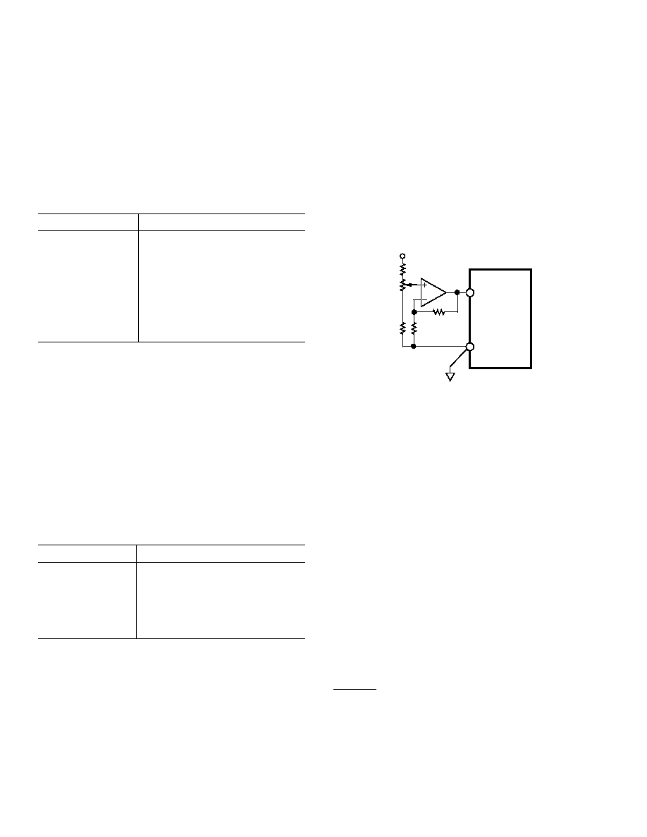
Figure 4 shows a circuit that can be used to adjust the offset and
full-scale errors on the AD7862 (VA1 on the AD7862-10 version
is shown for example purposes only). Where adjustment is
required, offset error must be adjusted before full-scale error.
This is achieved by trimming the offset of the op amp driving
the analog input of the AD7862 while the input voltage is a
1/2 LSB below analog ground. The trim procedure is as follows:
apply a voltage of –2.44 mV (–1/2 LSB) at VA1 (see Figure 4)
and adjust the op amp offset voltage until the ADC output code
flickers between 1111 1111 1111 and 0000 0000 0000.
V1
R1
10k
R2
500
R3
10k
AGND
AD7862*
*ADDITIONAL PINS OMITTED FOR CLARITY
INPUT
RANGE =
±10V
10k
R5
10k
R4
VA1
Figure 4. Full-Scale Adjust Circuit
Gain error can be adjusted at either the first code transition
(ADC negative full scale) or the last code transition (ADC
positive full scale). The trim procedures for both cases are as
follows:
Positive Full-Scale Adjust
Apply a voltage of +9.9927 V (FS/2 – 3/2 LSBs) at VA1. Adjust
R2 until the ADC output code flickers between 0111 1111 1110
and 0111 1111 1111.
Negative Full-Scale Adjust
Apply a voltage of –9.9976 V (–FS + 1/2 LSB) at VA1 and adjust
R2 until the ADC output code flickers between 1000 0000 0000
and 1000 0000 0001.
An alternative scheme for adjusting full-scale error in systems
that use an external reference is to adjust the voltage at the
VREF pin until the full-scale error for any of the channels is
adjusted out. The good full-scale matching of the channels will
ensure small full-scale errors on the other channels.
TIMING AND CONTROL
Figure 5a shows the timing and control sequence required to
obtain optimum performance (Mode 1) from the AD7862. In
the sequence shown, a conversion is initiated on the falling edge
of CONVST. This places both track/holds into hold simulta-
neously, and new data from this conversion is available in the
output register of the AD7862 3.6
s later. The BUSY signal
indicates the end of conversion, and at this time the conversion
results for both inputs are available to be read. A second
conversion is then initiated. If the multiplexer select A0 is low,
the first and second read pulses after the first conversion accesses
the result from channel A (VA1 and VA2 respectively). The third
相关PDF资料 |
PDF描述 |
|---|---|
| MS3101A16S-4P | CONN RCPT 2POS FREE HNG W/PINS |
| AD7899BRZ-1 | IC ADC 14BIT 400KSPS 5V 28SOIC |
| MS3106A12S-3S | CONN PLUG 2POS STRAIGHT W/SCKT |
| AD9649BCPZ-20 | IC ADC 14BIT 20MSPS 32LFCSP |
| 97-3101A-14S-6S | CONN RECEPT CBL MNT 6POS W/SOCK |
相关代理商/技术参数 |
参数描述 |
|---|---|
| AD7862ANZ-3 | 制造商:Rochester Electronics LLC 功能描述: 制造商:Analog Devices 功能描述: |
| AD7862AR-10 | 功能描述:IC ADC 12BIT DUAL 250KSPS 28SOIC RoHS:否 类别:集成电路 (IC) >> 数据采集 - 模数转换器 系列:- 标准包装:1 系列:- 位数:14 采样率(每秒):83k 数据接口:串行,并联 转换器数目:1 功率耗散(最大):95mW 电压电源:双 ± 工作温度:0°C ~ 70°C 安装类型:通孔 封装/外壳:28-DIP(0.600",15.24mm) 供应商设备封装:28-PDIP 包装:管件 输入数目和类型:1 个单端,双极 |
| AD7862AR-10REEL | 制造商:Analog Devices 功能描述:ADC Dual SAR 250ksps 12-bit Parallel 28-Pin SOIC W T/R |
| AD7862AR-2 | 制造商:Analog Devices 功能描述:ADC Dual SAR 250ksps 12-bit Parallel 28-Pin SOIC W 制造商:Rochester Electronics LLC 功能描述:DUAL 12-BIT PARALLEL ADC I.C. - Bulk |
| AD7862AR-2REEL | 功能描述:IC ADC 12BIT DUAL 250KSPS 28SOIC RoHS:否 类别:集成电路 (IC) >> 数据采集 - 模数转换器 系列:- 标准包装:1,000 系列:- 位数:12 采样率(每秒):300k 数据接口:并联 转换器数目:1 功率耗散(最大):75mW 电压电源:单电源 工作温度:0°C ~ 70°C 安装类型:表面贴装 封装/外壳:24-SOIC(0.295",7.50mm 宽) 供应商设备封装:24-SOIC 包装:带卷 (TR) 输入数目和类型:1 个单端,单极;1 个单端,双极 |
发布紧急采购,3分钟左右您将得到回复。