- 您现在的位置:买卖IC网 > PDF目录10533 > AD7862ANZ-10 (Analog Devices Inc)IC ADC 12BIT DUAL 250KSPS 28DIP PDF资料下载
参数资料
| 型号: | AD7862ANZ-10 |
| 厂商: | Analog Devices Inc |
| 文件页数: | 16/16页 |
| 文件大小: | 0K |
| 描述: | IC ADC 12BIT DUAL 250KSPS 28DIP |
| 标准包装: | 13 |
| 位数: | 12 |
| 采样率(每秒): | 250k |
| 数据接口: | 并联 |
| 转换器数目: | 2 |
| 功率耗散(最大): | 75mW |
| 电压电源: | 模拟和数字 |
| 工作温度: | -40°C ~ 85°C |
| 安装类型: | 通孔 |
| 封装/外壳: | 28-DIP(0.600",15.24mm) |
| 供应商设备封装: | 28-PDIP |
| 包装: | 管件 |
| 输入数目和类型: | 4 个单端,双极 |
AD7862
–9–
REV. 0
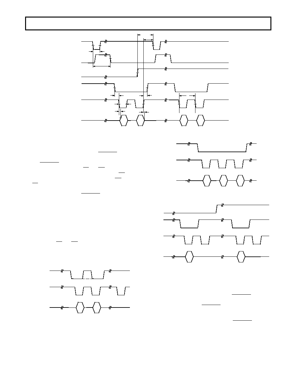
and fourth read pulses, after the second conversion and A0 high,
access the result from Channel B (VB1 and VB2 respectively). A0’s
state can be changed any time after the CONVST goes high,
i.e., track/holds into hold, and 400 ns prior to the next falling
edge of CONVST. Data is read from the part via a 12-bit
parallel data bus with standard CS and RD signal, i.e., the read
operation consists of a negative going pulse on the CS pin
combined with two negative going pulses on the RD pin (while
the CS is low), accessing the two 12-bit results. Once the read
operation has taken place, a further 300 ns should be allowed
before the next falling edge of CONVST to optimize the settling
of the track/hold amplifier before the next conversion is initiated.
With the internal clock frequency at its maximum (3.7 MHz—not
accessible externally), the achievable throughput rate for the
part is 3.6
s (conversion time) plus 100 ns (read time) plus
0.3
s (acquisition time). This results in a minimum throughput
time of 4
s (equivalent to a throughput rate of 250 kHz).
Read Options
Apart from the read operation described above and displayed in
Figure 5a, other CS and RD combinations can result in
different channels/inputs being read in different combinations.
Suitable combinations are shown in Figures 5b through 5d.
VA1
VA2
CS
RD
DATA
Figure 5b. Read Option A
VA1
VA2
CS
RD
DATA
VA1
Figure 5c. Read Option B
VA1
VB1
A0
CS
RD
DATA
Figure 5d. Read Option C
OPERATING MODES
Mode 1 Operation (High Sampling Performance)
The timing diagram in Figure 5a is for optimum performance in
operating mode 1 where the falling edge of CONVST starts
conversion and puts the track/hold amplifiers into their hold
mode. This falling edge of CONVST also causes the BUSY
signal to go high to indicate that a conversion is taking place.
The BUSY signal goes low when the conversion is complete,
which is 3.6
s max after the falling edge of CONVST, and new
data from this conversion is available in the output latch of the
AD7862. A read operation accesses this data. If the multiplexer
select A0 is low, the first and second read pulses after the first
conversion access the result from Channel A (VA1 and VA2
VA1
VA2
VB1
VB2
t
3
t
1
t
2
t
4
t
5
t
6
t
CONV = 3.6s
t7
CONVST
BUSY
A0
CS
RD
DATA
300ns
400ns
Figure 5a. Mode 1 Timing Operation Diagram for High Sampling Performance
相关PDF资料 |
PDF描述 |
|---|---|
| MS3101A16S-4P | CONN RCPT 2POS FREE HNG W/PINS |
| AD7899BRZ-1 | IC ADC 14BIT 400KSPS 5V 28SOIC |
| MS3106A12S-3S | CONN PLUG 2POS STRAIGHT W/SCKT |
| AD9649BCPZ-20 | IC ADC 14BIT 20MSPS 32LFCSP |
| 97-3101A-14S-6S | CONN RECEPT CBL MNT 6POS W/SOCK |
相关代理商/技术参数 |
参数描述 |
|---|---|
| AD7862ANZ-3 | 制造商:Rochester Electronics LLC 功能描述: 制造商:Analog Devices 功能描述: |
| AD7862AR-10 | 功能描述:IC ADC 12BIT DUAL 250KSPS 28SOIC RoHS:否 类别:集成电路 (IC) >> 数据采集 - 模数转换器 系列:- 标准包装:1 系列:- 位数:14 采样率(每秒):83k 数据接口:串行,并联 转换器数目:1 功率耗散(最大):95mW 电压电源:双 ± 工作温度:0°C ~ 70°C 安装类型:通孔 封装/外壳:28-DIP(0.600",15.24mm) 供应商设备封装:28-PDIP 包装:管件 输入数目和类型:1 个单端,双极 |
| AD7862AR-10REEL | 制造商:Analog Devices 功能描述:ADC Dual SAR 250ksps 12-bit Parallel 28-Pin SOIC W T/R |
| AD7862AR-2 | 制造商:Analog Devices 功能描述:ADC Dual SAR 250ksps 12-bit Parallel 28-Pin SOIC W 制造商:Rochester Electronics LLC 功能描述:DUAL 12-BIT PARALLEL ADC I.C. - Bulk |
| AD7862AR-2REEL | 功能描述:IC ADC 12BIT DUAL 250KSPS 28SOIC RoHS:否 类别:集成电路 (IC) >> 数据采集 - 模数转换器 系列:- 标准包装:1,000 系列:- 位数:12 采样率(每秒):300k 数据接口:并联 转换器数目:1 功率耗散(最大):75mW 电压电源:单电源 工作温度:0°C ~ 70°C 安装类型:表面贴装 封装/外壳:24-SOIC(0.295",7.50mm 宽) 供应商设备封装:24-SOIC 包装:带卷 (TR) 输入数目和类型:1 个单端,单极;1 个单端,双极 |
发布紧急采购,3分钟左右您将得到回复。