- 您现在的位置:买卖IC网 > PDF目录10102 > AD7865BSZ-3 (Analog Devices Inc)IC ADC 14BIT 4CHAN 5V 44-MQFP PDF资料下载
参数资料
| 型号: | AD7865BSZ-3 |
| 厂商: | Analog Devices Inc |
| 文件页数: | 7/19页 |
| 文件大小: | 0K |
| 描述: | IC ADC 14BIT 4CHAN 5V 44-MQFP |
| 标准包装: | 1 |
| 位数: | 14 |
| 采样率(每秒): | 350k |
| 数据接口: | 并联 |
| 转换器数目: | 1 |
| 功率耗散(最大): | 160mW |
| 电压电源: | 模拟和数字 |
| 工作温度: | -40°C ~ 85°C |
| 安装类型: | 表面贴装 |
| 封装/外壳: | 44-QFP |
| 供应商设备封装: | 44-MQFP(10x10) |
| 包装: | 托盘 |
| 输入数目和类型: | 4 个差分,双极 |
REV. B
AD7865
–15–
When operating the AD7865 in a standby mode between con-
versions, the power savings can be significant. For example,
with a throughput rate of 10 kSPS and external reference, the
AD7865 will be powered up 11
s out of every 100 s (1 s for
wake-up time and 9.6
s to convert four channels. Therefore,
the average power consumption drops to (115 mW
× 10.6%) or
12.2 mW approximately.
OFFSET AND FULL-SCALE ADJUSTMENT
In most Digital Signal Processing (DSP) applications, offset and
full-scale errors have little or no effect on system performance.
Offset error can always be eliminated in the analog domain by
ac coupling. Full-scale error effect is linear and does not cause
problems as long as the input signal is within the full dynamic
range of the ADC. Invariably, some applications will require
that the input signal span the full analog input dynamic range.
In such applications, offset and full-scale error will have to be
adjusted to zero.
Figure 13 shows a typical circuit that can be used to adjust the
offset and full-scale errors on the AD7865 (V1 on the AD7865-1
version is shown for example purposes only). Where adjustment
is required, offset error must be adjusted before full-scale error.
This is achieved by trimming the offset of the op amp driving
the analog input of the AD7865 while the input voltage is
1/2 LSB below analog ground. The trim procedure is as follows:
apply a voltage of –610
V (–1/2 LSB) at V1 and adjust the op
amp offset voltage until the ADC output code flickers between
1111 1111 1111 and 0000 0000 0000.
Gain error can be adjusted at either the first code transition
(ADC negative full scale) or the last code transition (ADC posi-
tive full scale). The trim procedures for both cases are as follows.
V1
R1
10k
R2
500
R3
10k
AGND
AD7865*
*ADDITIONAL PINS OMITTED FOR CLARITY
INPUT
RANGE =
10V
R5
10k
VINxA
R4
10k
Figure 13. Full-Scale Adjust Circuit
Positive Full-Scale Adjust
Apply a voltage of 9.9982 V (FS/2 – 3/2 LSB) at V1. Adjust R2
until the ADC output code flickers between 01 1111 1111 1110
and 01 1111 1111 1111.
Negative Full-Scale Adjust
Apply a voltage of –9.9998 V (–FS + 1/2 LSB) at V1 and adjust
R2 until the ADC output code flickers between 10 0000 0000
0000 and 10 0000 0000 0001.
An alternative scheme for adjusting full-scale error in systems
that use an external reference is to adjust the voltage at the VREF
pin until the full-scale error for any of the channels is adjusted
out. The good full-scale matching of the channels will ensure
small full-scale errors on the other channels.
DYNAMIC SPECIFICATIONS
The AD7865 is specified and 100% tested for dynamic perfor-
mance specifications as well as traditional dc specifications such
as Integral and Differential Nonlinearity. These ac specifications
are required for such signal processing applications as phased array
sonar, adaptive filters and spectrum analysis. These applications
require information on the ADC’s effect on the spectral content
of the input signal. Hence, the parameters for which the AD7865
is specified include SNR, harmonic distortion, intermodulation
distortion and peak harmonics. These terms are discussed in
more detail in the following sections.
Signal-to-Noise Ratio (SNR)
SNR is the measured signal-to-noise ratio at the output of the
ADC. The signal is the rms magnitude of the fundamental.
Noise is the rms sum of all the nonfundamental signals up to
half the sampling frequency (fS/2) excluding dc. SNR is depen-
dent upon the number of quantization levels used in the digitization
process; the more levels, the smaller the quantization noise. The
theoretical signal to noise ratio for a sine wave input is given by
SNR = (6.02N + 1.76) dB
(1)
where N is the number of bits.
Thus for an ideal 14-bit converter, SNR = 86.04 dB.
Figure 14 shows a histogram plot for 8192 conversions of a dc
input using the AD7865 with 5 V supply. The analog input was
set at the center of a code transition. It can be seen that most of
the codes appear in the one output bin, indicating very good
noise performance from the ADC.
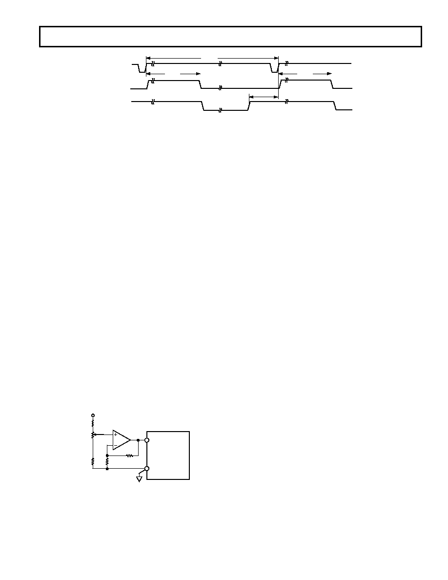
CONVST
BUSY
STBY
100 s
IDD = 3 A
tBUSY
t
WAKEUP
tBUSY
7 s
Figure 12. Power-Down between Conversion Sequences
相关PDF资料 |
PDF描述 |
|---|---|
| VE-24X-MX-F3 | CONVERTER MOD DC/DC 5.2V 75W |
| MS27472E18B32S | CONN RCPT 32POS WALL MT W/SCKT |
| VE-24X-MX-F2 | CONVERTER MOD DC/DC 5.2V 75W |
| D38999/20MC98PD | CONN RCPT 10POS WALL MNT W/PINS |
| VE-24X-MX-F1 | CONVERTER MOD DC/DC 5.2V 75W |
相关代理商/技术参数 |
参数描述 |
|---|---|
| AD7865BSZ-3REEL | 功能描述:IC ADC 14BIT 4CHAN 5V 44-MQFP RoHS:是 类别:集成电路 (IC) >> 数据采集 - 模数转换器 系列:- 标准包装:1 系列:- 位数:14 采样率(每秒):83k 数据接口:串行,并联 转换器数目:1 功率耗散(最大):95mW 电压电源:双 ± 工作温度:0°C ~ 70°C 安装类型:通孔 封装/外壳:28-DIP(0.600",15.24mm) 供应商设备封装:28-PDIP 包装:管件 输入数目和类型:1 个单端,双极 |
| AD7865YS-1 | 制造商:AD 制造商全称:Analog Devices 功能描述:Four-Channel, Simultaneous Sampling, Fast, 14-Bit ADC |
| AD7865YS-1REEL | 制造商:Analog Devices 功能描述:ADC Single SAR 350ksps 14-bit Parallel 44-Pin MQFP T/R |
| AD7865YS-2 | 制造商:Analog Devices 功能描述:ADC Single SAR 350ksps 14-bit Parallel 44-Pin MQFP 制造商:Rochester Electronics LLC 功能描述:4 CH. SIMULTANEOUS BIPOLAR,14-B ADC I.C. - Bulk |
| AD7865YS-3 | 制造商:Analog Devices 功能描述:ADC Single SAR 350ksps 14-bit Parallel 44-Pin MQFP |
发布紧急采购,3分钟左右您将得到回复。