参数资料
| 型号: | AD7869JRZ |
| 厂商: | Analog Devices Inc |
| 文件页数: | 13/16页 |
| 文件大小: | 0K |
| 描述: | IC I/O PORT 14BIT ANLG 28SOIC |
| 标准包装: | 1 |
| 应用: | 模拟 I/O |
| 接口: | TTL/CMOS |
| 电源电压: | 4.75 V ~ 5.25 V |
| 封装/外壳: | 28-SOIC(0.295",7.50mm 宽) |
| 供应商设备封装: | 28-SOIC W |
| 包装: | 管件 |
| 安装类型: | 表面贴装 |
AD7869
–6–
CONVERTER DETAILS
The AD7869 is a complete 14-bit I/O port; the only external
components required for normal operation are pull-up resistors
for the ADC data outputs, and power supply decoupling capaci-
tors. The AD7869 is comprised of a 14-bit successive approxi-
mation ADC with a track/hold amplifier, a 14-bit DAC with a
buffered output and two 3 V buried Zener references, a clock os-
cillator and control logic.
ADC CLOCK
The AD7869 has an internal clock oscillator that can be used for
the ADC conversion procedure. The oscillator is enabled by ty-
ing the CLK input to VSS. The oscillator is laser trimmed at the
factory to give a maximum conversion time of 10
s. The mark/
space ratio can vary from 40/60 to 60/40. Alternatively, an exter-
nal TTL compatible clock may be applied to this input. The al-
lowable mark/space ratio of an external clock is 40/60 to 60/40.
RCLK is a clock output, used for the serial interface. This out-
put is derived directly from the ADC clock source and can be
switched off at the end of conversion with the CONTROL
input.
ADC CONVERSION TIMING
The conversion time for both external clock and continuous in-
ternal clock can vary from 19 to 20 rising clock edges, depending
on the conversion start to ADC clock synchronization. If a con-
version is initiated within 30 ns prior to a rising edge of the ADC
clock, the conversion time will consist of 20 rising clock edges,
i.e., 9.5
s conversion time. For noncontinuous internal clock,
the conversion time always consists of 19 rising clock edges.
ADC TRACK-AND-HOLD AMPLIFIER
The track-and-hold amplifier on the analog input of the AD7869
allows the ADC to accurately convert an input sine wave of 6 V
peak–peak amplitude to 14-bit accuracy. The input impedance is
typically 9 k
; an equivalent circuit is shown in Figure 1. The
input bandwidth of the track/hold amplifier is much greater
than the Nyquist rate of the ADC even when the ADC is oper-
ated at its maximum throughput rate. The 0.1 dB cutoff fre-
quency occurs typically at 500 kHz. The track/hold amplifier
acquires an input signal to 14-bit accuracy in less than 2
s. The
overall throughput rate is equal to the conversion time plus the
track/hold amplifier acquisition time. For a 2.0 MHz input clock,
the throughput time is 12
s max.
AD7869*
4.5k
4.5k
*ADDITIONAL PINS OMITTED FOR CLARITY
VIN
TO INTERNAL
COMPARATOR
TRACK/HOLD
AMPLIFIER
TO INTERNAL
3V REFERENCE
Figure 1. ADC Analog Input
The operation of the track/hold amplifier is essentially transpar-
ent to the user. The track/hold amplifier goes from its track
mode to its hold mode at the start of conversion on the rising
edge of
CONVST.
INTERNAL REFERENCES
The AD7869 has two on-chip temperature compensated buried
Zener references that are factory trimmed to 3 V
±10 mV. One
reference provides the appropriate biasing for the ADC, while
the other is available as a reference for the DAC. Both reference
outputs are available (labelled RO DAC and RO ADC) and are
capable of providing up to 500
A to an external load.
The DAC input reference (RI DAC) can be sourced externally
or connected to any of the two on-chip references. Applications
requiring good full-scale error matching between the DAC and
the ADC should use the ADC reference as shown in Figure 4.
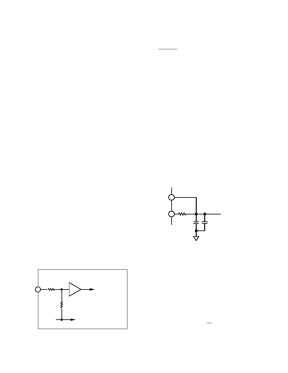
The maximum recommended capacitance on either of the refer-
ence output pins for normal operation is 50 pF. If either of the
reference outputs is required to drive a capacitive load greater
than 50 pF, then a 200
resistor must be placed in series with
the capacitive load. The addition of decoupling capacitors,
10
F in parallel with 0.1 F as shown in Figure 2, improves
noise performance. The improvement in noise performance can
be seen from the graph in Figure 3. Note: this applies for the
DAC output only; reference decoupling components do not af-
fect ADC performance. Consequently, a typical application will
have just the DAC reference decoupled with the other one open
circuited.
RI DAC
200
RO DAC
or
RO ADC*
EXT LOAD
GREATER THAN 50pF
*RO DAC/RO ADC CAN BE LEFT
OPEN CIRCUIT IF NOT USED
10
F
0.1
F
Figure 2. Reference Decoupling Components
DAC OUTPUT AMPLIFIER
The output from the voltage mode DAC is buffered by a non-
inverting amplifier. The buffer amplifier is capable of developing
±3 V across 2 k and 100 pF load to ground and can produce
6 V peak-to-peak sine wave signals to a frequency of 20 kHz.
The output is updated on the falling edge of the LDAC input.
The output voltage settling time, to within 1/2 LSB of its final
value, is typically less than 3.5
s.
The small signal (200 mV p–p) bandwidth of the output buffer
amplifier is typically 1 MHz. The output noise from the ampli-
fier is low with a figure of 30 nV/
√Hz at a frequency of 1 kHz.
The broadband noise from the amplifier exhibits a typical peak-
to-peak figure of 150
V for a 1 MHz output bandwidth. Figure
3 shows a typical plot of noise spectral density versus frequency
for the output buffer amplifier and for either of the on-chip
references.
REV. B
相关PDF资料 |
PDF描述 |
|---|---|
| AD7874SE | IC DAS 12BIT 4CH 5V 28-CLCC |
| AD7890BRZ-4 | IC DAS 12BIT 8CH 24-SOIC |
| AD7891BPZ-2 | IC DAS 12BIT 8CH 44-PLCC |
| AD80066KRSZRL | IC DSP CTLR 16BIT 28SSOP |
| AD8016AREZ-REEL7 | IC LINE DRIVER ADSL 28TSSOP |
相关代理商/技术参数 |
参数描述 |
|---|---|
| AD7870 | 制造商:AD 制造商全称:Analog Devices 功能描述:LC2MOS Complete, 12-Bit, 100 kHz, Sampling ADCs |
| AD7870A | 制造商:AD 制造商全称:Analog Devices 功能描述:LC2MOS Complete, 12-Bit, 100 kHz , Sampling ADC |
| AD7870AJN | 制造商:Analog Devices 功能描述:ADC Single SAR 100ksps 12-bit Parallel/Serial 24-Pin PDIP 制造商:Rochester Electronics LLC 功能描述:12-BIT SAMPLING ADC IC - Bulk |
| AD7870AJNZ | 功能描述:IC ADC 12BIT SAMPLING 3V 24-DIP RoHS:是 类别:集成电路 (IC) >> 数据采集 - 模数转换器 系列:- 标准包装:1 系列:- 位数:14 采样率(每秒):83k 数据接口:串行,并联 转换器数目:1 功率耗散(最大):95mW 电压电源:双 ± 工作温度:0°C ~ 70°C 安装类型:通孔 封装/外壳:28-DIP(0.600",15.24mm) 供应商设备封装:28-PDIP 包装:管件 输入数目和类型:1 个单端,双极 |
| AD7870AQ | 功能描述:IC ADC 12BIT SAMPLING 3V 24-CDIP RoHS:否 类别:集成电路 (IC) >> 数据采集 - 模数转换器 系列:- 产品培训模块:Lead (SnPb) Finish for COTS Obsolescence Mitigation Program 标准包装:2,500 系列:- 位数:12 采样率(每秒):3M 数据接口:- 转换器数目:- 功率耗散(最大):- 电压电源:- 工作温度:- 安装类型:表面贴装 封装/外壳:SOT-23-6 供应商设备封装:SOT-23-6 包装:带卷 (TR) 输入数目和类型:- |
发布紧急采购,3分钟左右您将得到回复。