- 您现在的位置:买卖IC网 > PDF目录10055 > AD7876CR (Analog Devices Inc)IC ADC 12BIT SAMPLING 10V 24SOIC PDF资料下载
参数资料
| 型号: | AD7876CR |
| 厂商: | Analog Devices Inc |
| 文件页数: | 3/28页 |
| 文件大小: | 0K |
| 描述: | IC ADC 12BIT SAMPLING 10V 24SOIC |
| 产品变化通告: | Conversion Time Change |
| 标准包装: | 1 |
| 位数: | 12 |
| 采样率(每秒): | 100k |
| 数据接口: | 串行,并联 |
| 转换器数目: | 1 |
| 功率耗散(最大): | 95mW |
| 电压电源: | 双 ± |
| 工作温度: | -40°C ~ 85°C |
| 安装类型: | 表面贴装 |
| 封装/外壳: | 24-SOIC(0.295",7.50mm 宽) |
| 供应商设备封装: | 24-SOIC W |
| 包装: | 管件 |
| 输入数目和类型: | 1 个单端,双极 |
第1页第2页当前第3页第4页第5页第6页第7页第8页第9页第10页第11页第12页第13页第14页第15页第16页第17页第18页第19页第20页第21页第22页第23页第24页第25页第26页第27页第28页
AD7870/AD7875/AD7876
Rev. C | Page 11 of
28
CONVERTER DETAILS
The AD7870/AD7875/AD7876 is a complete 12-bit ADC,
requiring no external components apart from power supply
decoupling capacitors. It is comprised of a 12-bit successive
approximation ADC based on a fast settling voltage output
DAC, a high speed comparator and SAR, a track-and-hold
amplifier, a 3 V buried Zener reference, a clock oscillator,
and control logic.
INTERNAL REFERENCE
The AD7870/AD7875/AD7876 have on-chip temperature
compensated buried Zener reference that is factory trimmed
to 3 V ± 10 mV. Internally it provides both the DAC reference
and the dc bias required for bipolar operation (AD7870 and
AD7876). The reference output is available (REF OUT) and
capable of providing up to 500 μA to an external load.
The maximum recommended capacitance on REF OUT for
normal operation is 50 pF. If the reference is required for use
external to the ADC, it should be decoupled with a 200 Ω
resistor in series with a parallel combination of a 10 μF
tantalum capacitor and a 0.1 μF ceramic capacitor. These
decoupling components are required to remove voltage
spikes caused by the ADC’s internal operation.
TEMPERATURE
COMPENSATION
AD7870/AD7875/AD7876
REF OUT
VSS
VDD
07
73
0-
00
6
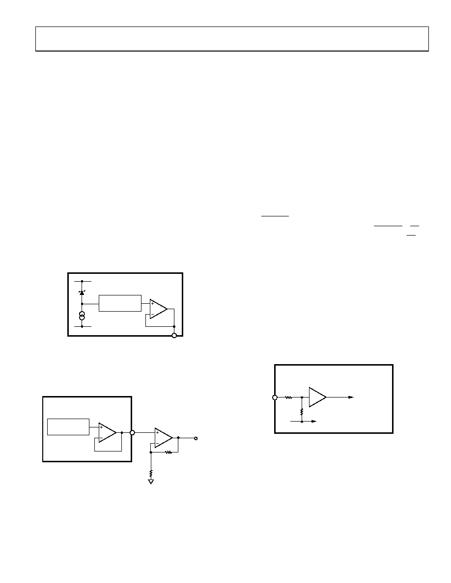
Figure 6. Reference Circuit
The reference output voltage is 3 V. For applications using the
AD7875 or AD7876, a 5 V or 10 V reference may be required.
Figure 7 shows how to scale the 3 V REF OUT voltage to
provide either a 5 V or 10 V external reference.
INTERNAL 3V
REFERENCE
AD7870/AD7875/AD7876
REF OUT
15k
(3.9k)
10k
(9.1k)
VOUT = 5V (10V)
07
73
0-
0
07
Figure 7. Generating a 5 V or 10 V Reference
TRACK-AND-HOLD AMPLIFIER
The track-and-hold amplifier on the analog input of the
AD7870/AD7875/AD7876 allows the ADC to accurately
convert input frequencies to 12-bit accuracy. The input
bandwidth of the track-and-hold amplifier is much greater
than the Nyquist rate of the ADC even when the ADC is
operated at its maximum throughput rate. The 0.1 dB cutoff
frequency occurs typically at 500 kHz. The track-and-hold
amplifier acquires an input signal to 12-bit accuracy in less than
2 μs. The overall throughput rate is equal to the conversion time
plus the track-and-hold amplifier acquisition time. For a 2.5 MHz
input clock the throughput rate is 10 μs max.
The operation of the track-and-hold is essentially transparent
to the user. The track-and-hold amplifier goes from its tracking
mode to its hold mode at the start of conversion.
If the CONVST input is used to start conversion then the track
to hold transition occurs on the rising edge of CONVST. If CS
starts conversion, this transition occurs on the falling edge of CS.
ANALOG INPUT
The three parts differ from each other in the analog input
voltage range that they can handle. The AD7870 accepts ±3 V
input signals, the AD7876 accepts a ±10 V input range, while
the input range for the AD7875 is 0 V to +5 V.
Figure 8 shows the AD7870 analog input. The analog input
range is ±3 V into an input resistance of typically 15 kΩ. The
designed code transitions occur midway between successive
integer LSB values (that is, 1/2 LSB, 3/2 LSBs, 5/2 LSBs . . .
FS–3/2 LSBs). The output code is twos complement binary with
1 LSB = FS/4096 = 6 V/4096 = 1.46 mV. The ideal input/output
transfer function is shown in Figure 11.
AD7870
TRACK-AND-HOLD
AMPLIFIER
TO INTERNAL
3V REFERENCE
R
TO INTERNAL
COMPARATOR
07
73
0-
00
8
Figure 8. AD7970 Analog Input
The AD7876 analog input structure is shown in Figure 9. The
analog input range is ±10 V into an input resistance of typically
33 kΩ. As before, the designed code transitions occur midway
between successive integer LSB values. The output code is twos
complement with 1 LSB = FS/4096 = 20 V/4096 = 4.88 mV. The
ideal input/output transfer function is shown in Figure 11.
相关PDF资料 |
PDF描述 |
|---|---|
| VE-264-MX-F2 | CONVERTER MOD DC/DC 48V 75W |
| MS27474E20A41P | CONN RCPT 41POS JAM NUT W/PINS |
| AD7572JN12 | IC ADC 12BIT HS LC2MOS 24-DIP |
| VE-264-MX-F1 | CONVERTER MOD DC/DC 48V 75W |
| MS3101R12-5P | CONN RCPT 1POS PANEL MNT W/PINS |
相关代理商/技术参数 |
参数描述 |
|---|---|
| AD7876CR-REEL | 功能描述:IC ADC 12BIT SAMPLING 10V 24SOIC RoHS:否 类别:集成电路 (IC) >> 数据采集 - 模数转换器 系列:- 标准包装:1 系列:- 位数:14 采样率(每秒):83k 数据接口:串行,并联 转换器数目:1 功率耗散(最大):95mW 电压电源:双 ± 工作温度:0°C ~ 70°C 安装类型:通孔 封装/外壳:28-DIP(0.600",15.24mm) 供应商设备封装:28-PDIP 包装:管件 输入数目和类型:1 个单端,双极 |
| AD7876CRZ | 功能描述:IC ADC 12BIT SAMPLING 10V 24SOIC RoHS:是 类别:集成电路 (IC) >> 数据采集 - 模数转换器 系列:- 标准包装:1 系列:- 位数:14 采样率(每秒):83k 数据接口:串行,并联 转换器数目:1 功率耗散(最大):95mW 电压电源:双 ± 工作温度:0°C ~ 70°C 安装类型:通孔 封装/外壳:28-DIP(0.600",15.24mm) 供应商设备封装:28-PDIP 包装:管件 输入数目和类型:1 个单端,双极 |
| AD7876CRZ1 | 制造商:AD 制造商全称:Analog Devices 功能描述:LC2MOS Complete, 12-Bit, 100 kHz, Sampling ADCs |
| AD7876TQ | 制造商:Analog Devices 功能描述:ADC Single SAR 100ksps 12-bit Parallel/Serial 24-Pin CDIP 制造商:Analog Devices 功能描述:ADC SGL SAR 100KSPS 12-BIT PARALLEL/SERL 24CDIP - Rail/Tube 制造商:Rochester Electronics LLC 功能描述:12-BIT SAMPLING ADC IC - Bulk 制造商:Analog Devices 功能描述:IC ADC 12BIT SAMPLING 10V 24CDIP 制造商:Analog Devices Inc. 功能描述:Analog to Digital Converters - ADC 12-BIT SAMPLING ADC IC 制造商:Analog Devices 功能描述:CONVERTER - ADC |
| AD7876TQ/883B | 制造商:未知厂家 制造商全称:未知厂家 功能描述:Analog-to-Digital Converter, 12-Bit |
发布紧急采购,3分钟左右您将得到回复。