- 您现在的位置:买卖IC网 > PDF目录10055 > AD7876CR (Analog Devices Inc)IC ADC 12BIT SAMPLING 10V 24SOIC PDF资料下载
参数资料
| 型号: | AD7876CR |
| 厂商: | Analog Devices Inc |
| 文件页数: | 13/28页 |
| 文件大小: | 0K |
| 描述: | IC ADC 12BIT SAMPLING 10V 24SOIC |
| 产品变化通告: | Conversion Time Change |
| 标准包装: | 1 |
| 位数: | 12 |
| 采样率(每秒): | 100k |
| 数据接口: | 串行,并联 |
| 转换器数目: | 1 |
| 功率耗散(最大): | 95mW |
| 电压电源: | 双 ± |
| 工作温度: | -40°C ~ 85°C |
| 安装类型: | 表面贴装 |
| 封装/外壳: | 24-SOIC(0.295",7.50mm 宽) |
| 供应商设备封装: | 24-SOIC W |
| 包装: | 管件 |
| 输入数目和类型: | 1 个单端,双极 |
第1页第2页第3页第4页第5页第6页第7页第8页第9页第10页第11页第12页当前第13页第14页第15页第16页第17页第18页第19页第20页第21页第22页第23页第24页第25页第26页第27页第28页
AD7870/AD7875/AD7876
Rev. C | Page 20 of 2
8
This is a two-byte read instruction. During the first read
operation BUSY, in conjunction with CS, forces the micro-
processor to WAIT for the ADC conversion. At the end of
conversion the ADC low byte (DB7 – DB0) is loaded into
D15 – D8 of the D0 register and the ADC high byte (DB15 –
DB7) is loaded into Bits D7 – D0 of the D0 register.
The following rotate instruction to the D0 register swaps the
high and low bytes to the correct format.
R0L = 8, D0.
Note that while executing the two-byte read instruction above,
WAIT states are inserted during the first read operation only
and not for the second.
A15
A0
CONVST
CS
HBEN
A0
12/8/CLK
BUSY/INT
RD
DB7
C
R2
DB0
ADDRESS BUS
DATA BUS
ADDR
DECODE
EN
DTACK
AS
STRB
D15
D0
R/W
07
73
0-
0
25
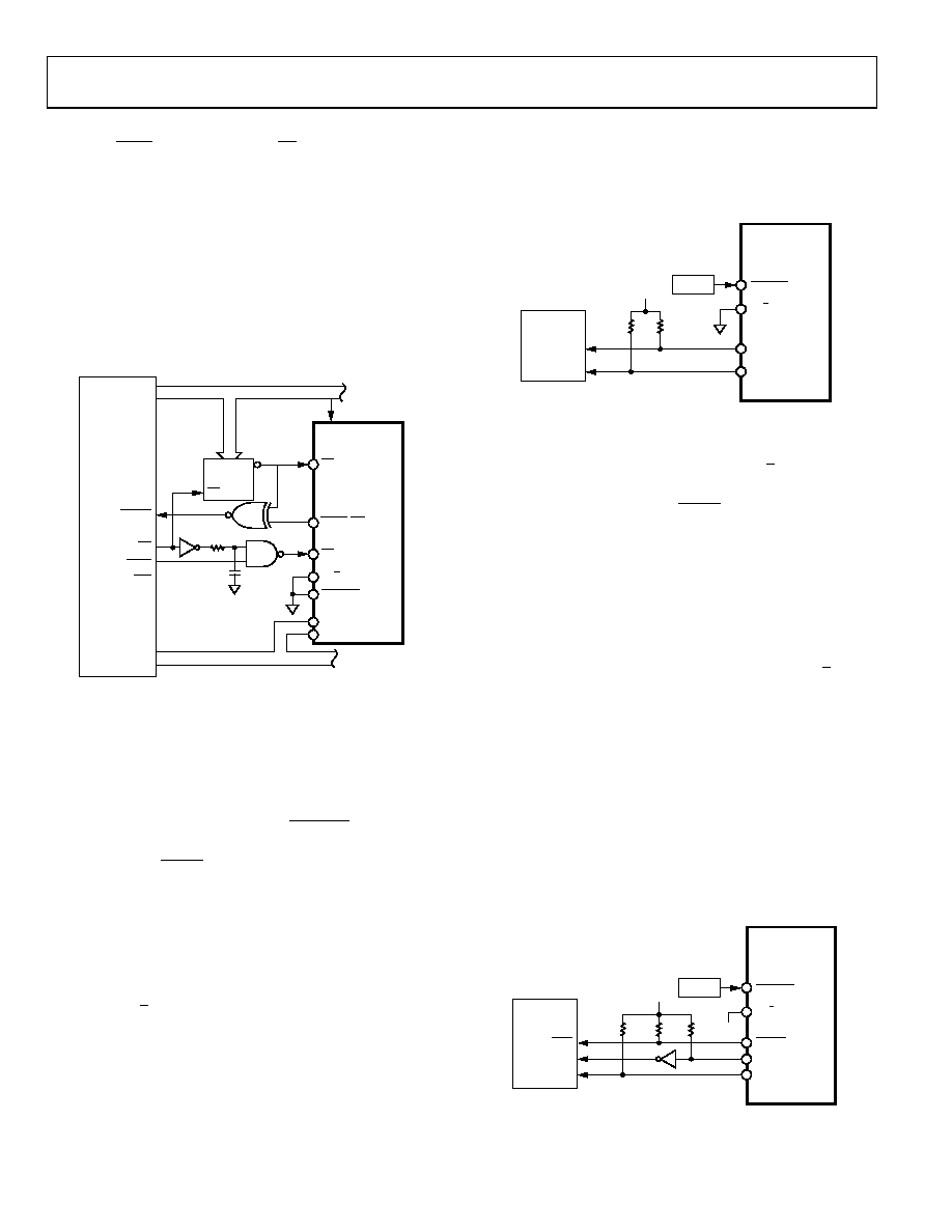
1ADDITIONAL PINS OMITTED FOR CLARITY.
2RESISTOR AND CAPACITOR REQUIRED TO GUARANTEE
t15.
AD7870/
AD7875/
AD78761
MC68008
Figure 25. MC68008 Byte Interface
SERIAL INTERFACING
AD7870/AD7875/AD7876 configured for serial interfacing. In
all four interfaces, the ADC is configured for Mode 1 operation.
The interfaces show a timer driving the CONVST input, but
this could be generated from a decoded address if required. The
SCLK, SDAT and SSTRB are open-drain outputs. If these are
required to drive capacitive loads in excess 35 pF, buffering is
recommended.
DSP56000 Serial Interface
Figure 26 shows a serial interface between the AD7870/AD7875/
AD7876, and the DSP56000. The interface arrangement is
two-wire with the ADC configured for noncontinuous clock
operation (12/8/CLK = 0 V). The DSP56000 is configured
for normal mode asynchronous operation with gated clock.
It is also set up for a 16-bit word with SCK and SC1 as inputs
and the FSL control bit set to a 0. In this configuration, the
DSP56000 assumes valid data on the first falling edge of SCK.
Since the ADC provides valid data on this first edge, there is
no need for a strobe or framing pulse for the data. SCLK and
SDATA are gated off when the ADC is not performing a
conversion. During conversion, data is valid on the SDATA
output of the ADC and is clocked into the receive data shift
register of the DSP56000. When this register has received
16 bits of data, it generates an internal interrupt on the
DSP56000 to read the data from the register.
CONVST
12/8/CLK
SCLK
2k
5V
4.7k
SDATA
SCK
SRD
DSP56000
07
73
0-
0
26
TIMER
1ADDITIONAL PINS OMITTED FOR CLARITY.
AD7870/
AD7875/
AD78761
Figure 26. DSP56000 Serial Interface
The DSP56000 and AD7870/AD7875/AD7876 can also be
configured for continuous clock operation (12/8/CLK = 5 V).
In this case, a strobe pulse is required by the DSP56000 to
indicate when data is valid. The SSTRB output of the ADC
is inverted and applied to the SC1 input of the DSP56000 to
provide this strobe pulse. All other conditions and connections
are the same as for gated clock operation.
NEC7720/77230 Serial Interface
A serial interface between the AD7870/AD7875/AD7876 and
the NEC7720 is shown in Figure 27. In the interface shown, the
ADC is configured for continuous clock operation. This can be
changed to a noncontinuous clock by simply tying the 12/8/CLK
input of the ADC to 0 V with all other connections remaining
the same. The NEC7720 expects valid data on the rising edge of
its SCK input and therefore an inverter is required on the SCLK
output of the ADC. The NEC7720 is configured for a 16-bit
data word. Once the 16 bits of data have been received by the SI
register of the NEC7720, an internal interrupt is generated to
read the contents of the SI register.
The NEC77230 interface is similar to that just outlined for the
NEC7720. However, the clock input of the NEC77230 is SICLK.
Additionally, no inverter is required between the ADC SCLK
output and this SICLK input since the NEC77230 assumes data
is valid on the falling edge of SICLK.
CONVST
12/8/CLK
2k
+5V
–5V
4.7k
SCLK
SIEN
SI
SCLK
SSTRB
SDATA
PD7720
07
73
0-
02
7
TIMER
1ADDITIONAL PINS OMITTED FOR CLARITY.
AD7870/
AD7875/
AD78761
Figure 27. NEC7720 Serial Interface
相关PDF资料 |
PDF描述 |
|---|---|
| VE-264-MX-F2 | CONVERTER MOD DC/DC 48V 75W |
| MS27474E20A41P | CONN RCPT 41POS JAM NUT W/PINS |
| AD7572JN12 | IC ADC 12BIT HS LC2MOS 24-DIP |
| VE-264-MX-F1 | CONVERTER MOD DC/DC 48V 75W |
| MS3101R12-5P | CONN RCPT 1POS PANEL MNT W/PINS |
相关代理商/技术参数 |
参数描述 |
|---|---|
| AD7876CR-REEL | 功能描述:IC ADC 12BIT SAMPLING 10V 24SOIC RoHS:否 类别:集成电路 (IC) >> 数据采集 - 模数转换器 系列:- 标准包装:1 系列:- 位数:14 采样率(每秒):83k 数据接口:串行,并联 转换器数目:1 功率耗散(最大):95mW 电压电源:双 ± 工作温度:0°C ~ 70°C 安装类型:通孔 封装/外壳:28-DIP(0.600",15.24mm) 供应商设备封装:28-PDIP 包装:管件 输入数目和类型:1 个单端,双极 |
| AD7876CRZ | 功能描述:IC ADC 12BIT SAMPLING 10V 24SOIC RoHS:是 类别:集成电路 (IC) >> 数据采集 - 模数转换器 系列:- 标准包装:1 系列:- 位数:14 采样率(每秒):83k 数据接口:串行,并联 转换器数目:1 功率耗散(最大):95mW 电压电源:双 ± 工作温度:0°C ~ 70°C 安装类型:通孔 封装/外壳:28-DIP(0.600",15.24mm) 供应商设备封装:28-PDIP 包装:管件 输入数目和类型:1 个单端,双极 |
| AD7876CRZ1 | 制造商:AD 制造商全称:Analog Devices 功能描述:LC2MOS Complete, 12-Bit, 100 kHz, Sampling ADCs |
| AD7876TQ | 制造商:Analog Devices 功能描述:ADC Single SAR 100ksps 12-bit Parallel/Serial 24-Pin CDIP 制造商:Analog Devices 功能描述:ADC SGL SAR 100KSPS 12-BIT PARALLEL/SERL 24CDIP - Rail/Tube 制造商:Rochester Electronics LLC 功能描述:12-BIT SAMPLING ADC IC - Bulk 制造商:Analog Devices 功能描述:IC ADC 12BIT SAMPLING 10V 24CDIP 制造商:Analog Devices Inc. 功能描述:Analog to Digital Converters - ADC 12-BIT SAMPLING ADC IC 制造商:Analog Devices 功能描述:CONVERTER - ADC |
| AD7876TQ/883B | 制造商:未知厂家 制造商全称:未知厂家 功能描述:Analog-to-Digital Converter, 12-Bit |
发布紧急采购,3分钟左右您将得到回复。