- 您现在的位置:买卖IC网 > PDF目录10043 > AD7878JNZ (Analog Devices Inc)IC ADC 12BIT W/DSP INT 28-DIP PDF资料下载
参数资料
| 型号: | AD7878JNZ |
| 厂商: | Analog Devices Inc |
| 文件页数: | 10/16页 |
| 文件大小: | 0K |
| 描述: | IC ADC 12BIT W/DSP INT 28-DIP |
| 标准包装: | 1 |
| 位数: | 12 |
| 采样率(每秒): | 100k |
| 数据接口: | DSP |
| 转换器数目: | 1 |
| 功率耗散(最大): | 95.5mW |
| 电压电源: | 模拟和数字,双 ± |
| 工作温度: | 0°C ~ 70°C |
| 安装类型: | 通孔 |
| 封装/外壳: | 28-DIP(0.600",15.24mm) |
| 供应商设备封装: | 28-PDIP |
| 包装: | 管件 |
| 输入数目和类型: | 1 个单端,双极 |
AD7878
–3–
REV. A
Limit at TMIN, TMAX
Parameter
(L Grade)
(J, K, A, B Grades)
(S Grade)
Units
Conditions/Comments
tl
65
75
ns max
CLK IN to
BUSY Low Propagation Delay
t2
65
75
ns max
CLK IN to
BUSY High Propagation Delay
t3
2 CLK IN Cycles
min
CONVST Pulse Width
t4
0
ns min
CS to DMRD/REGISTER ENABLE Setup Time
t5
0
ns min
CS to DMRD/ REGISTER ENABLE Hold Time
t6
45
60
ns min
DMRD Pulse Width
50
s max
t7
16
ns min
ADD0 to
DMRD/REGISTER ENABLE Setup Time
t8
0
ns min
ADD0 to
DMRD/REGISTER ENABLE Hold Time
t9
2
41
57
ns min
Data Access Time after
DMRD
t10
3
5
ns min
Bus Relinquish Time
45
ns max
t11
42
55
ns min
REGISTER ENABLE Pulse Width
50
s max
t12
20
30
ns min
Data Valid to REGISTER ENABLE Setup Time
t13
10
ns min
Data Hold Time after REGISTER ENABLE
t14
2
41
57
ns min
Data Access Time after BUSY
tRESET
2 CLK IN Cycles
min
RESET Pulse Width
NOTES
1Timing Specifications in bold print are 100% production tested. All other times are sample tested at +25
°C to ensure compliance. All input signals are specified with
tr = tf = 5 ns (10% to 90% of 5 V) and timed from a voltage level of 1.6 V.
2t
9 and t14 are measured with the load circuits of Figure 1 and defined as the time required for an output to cross 0.8 V or 2.4 V.
3t
10 is defined as the time required for the data lines to change 0.5 V when loaded with the circuits of Figure 2.
Specifications subject to change without notice.
(VDD = 5 V
5%, VCC = 5 V
5%, VSS = –5 V
5%)
TIMING CHARACTERISTICS1
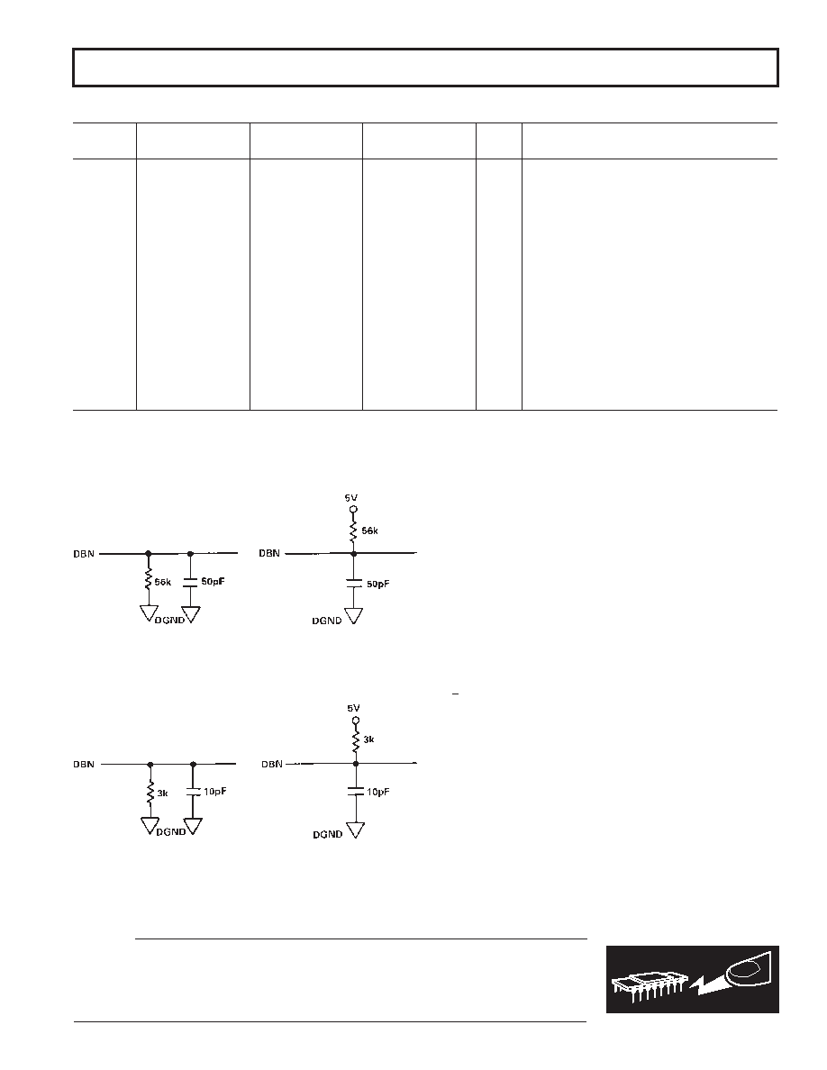
Figure 1. Load Circuits for Access Time
Figure 2. Load Circuits for Output Float Delay
ABSOLUTE MAXIMUM RATINGS*
(TA = +25°C unless otherwise stated)
VDD to DGND . . . . . . . . . . . . . . . . . . . . . . . . . –0.3 V to +7 V
VCC to DGND . . . . . . . . . . . . . . . . . . . . . . . . . –0.3 V to +7 V
VSS to DGND . . . . . . . . . . . . . . . . . . . . . . . . . +0.3 V to –7 V
VDD to VCC . . . . . . . . . . . . . . . . . . . . . . . . . . –0.3 V to +0.3 V
AGND to DGND . . . . . . . . . . . . . . . . . –0.3 V to VDD +0.3 V
VIN to AGND . . . . . . . . . . . . . . . . . . . . . . . . . –15 V to +15 V
REF OUT to AGND . . . . . . . . . . . . . . . . . . . . . . . . . 0 to VDD
Digital Inputs to DGND
CLK IN,
DMWR, DMRD, RESET,
CS, CONVST, ADD0 . . . . . . . . . . . . –0.3 V to V
DD +0.3 V
Digital Outputs to DGND
ALFL, BUSY . . . . . . . . . . . . . . . . . . –0.3 V to V
DD +0.3 V
Data Pins
DB11–DB0 . . . . . . . . . . . . . . . . . . . . –0.3 V to VDD +0.3 V
Operating Temperature Range
J, K, L Versions . . . . . . . . . . . . . . . . . . . . . . . 0
°C to +70°C
A, B Versions . . . . . . . . . . . . . . . . . . . . . . . –25
°C to +85°C
S Version . . . . . . . . . . . . . . . . . . . . . . . . . –55
°C to +125°C
Storage Temperature Range . . . . . . . . . . . . –65
°C to +150°C
Lead Temperature (Soldering, 10 sec) . . . . . . . . . . . . +300
°C
Power Dissipation (Any Package) to +75
°C . . . . . . 1000 mW
Derates above +75
°C by . . . . . . . . . . . . . . . . . . 10 mW/°C
*Stresses above those listed under Absolute Maximum Ratings may cause perma-
nent damage to the device. These are stress rating only; functional operation of the
device at these or any other conditions above those indicated in the operational
sections of this specification is not implied. Exposure to absolute maximum rating
conditions for extended periods may affect device reliability
WARNING!
ESD SENSITIVE DEVICE
CAUTION
ESD (electrostatic discharge) sensitive device. Electrostatic charges as high as 4000 V readily
accumulate on the human body and test equipment and can discharge without detection.
Although the AD7878 features proprietary ESD protection circuitry, permanent damage may
occur on devices subjected to high energy electrostatic discharges. Therefore, proper ESD
precautions are recommended to avoid performance degradation or loss of functionality.
a. High-Z to VOH
b. High-Z to VOL
a. VOH to High-Z
b. VOL to High-Z
相关PDF资料 |
PDF描述 |
|---|---|
| IDT72V801L15PFI8 | IC SYNC FIFO 256X9 15NS 64QFP |
| LTC1350ISW | IC TXRX 3.3V EIA/TIA-562 28-SOIC |
| VE-B6F-MW-F4 | CONVERTER MOD DC/DC 72V 100W |
| MS3106R28-11SX | CONN PLUG 22POS STRAIGHT W/SCKT |
| VI-B1Z-MX | CONVERTER MOD DC/DC 2V 30W |
相关代理商/技术参数 |
参数描述 |
|---|---|
| AD7878JP | 制造商:Analog Devices 功能描述:ADC Single SAR 100ksps 12-bit Parallel 28-Pin PLCC 制造商:Rochester Electronics LLC 功能描述:12-BIT ADC IC - Bulk |
| AD7878JPZ | 功能描述:IC ADC 12BIT W/DSP INT 28-PLCC RoHS:是 类别:集成电路 (IC) >> 数据采集 - 模数转换器 系列:- 产品培训模块:Lead (SnPb) Finish for COTS Obsolescence Mitigation Program 标准包装:2,500 系列:- 位数:12 采样率(每秒):3M 数据接口:- 转换器数目:- 功率耗散(最大):- 电压电源:- 工作温度:- 安装类型:表面贴装 封装/外壳:SOT-23-6 供应商设备封装:SOT-23-6 包装:带卷 (TR) 输入数目和类型:- |
| AD7878JPZ-REEL | 功能描述:IC ADC 12BIT W/DSP 28PLCC RoHS:是 类别:集成电路 (IC) >> 数据采集 - 模数转换器 系列:- 标准包装:1 系列:- 位数:14 采样率(每秒):83k 数据接口:串行,并联 转换器数目:1 功率耗散(最大):95mW 电压电源:双 ± 工作温度:0°C ~ 70°C 安装类型:通孔 封装/外壳:28-DIP(0.600",15.24mm) 供应商设备封装:28-PDIP 包装:管件 输入数目和类型:1 个单端,双极 |
| AD7878KN | 制造商:Analog Devices 功能描述:ADC Single SAR 100ksps 12-bit Parallel 28-Pin PDIP W 制造商:Rochester Electronics LLC 功能描述:COMPLETE 12 BIT ADC IC - Bulk |
| AD7878KP | 制造商:Rochester Electronics LLC 功能描述:12-BIT ADC IC - Bulk 制造商:Analog Devices 功能描述: |
发布紧急采购,3分钟左右您将得到回复。