- 您现在的位置:买卖IC网 > PDF目录10043 > AD7878JNZ (Analog Devices Inc)IC ADC 12BIT W/DSP INT 28-DIP PDF资料下载
参数资料
| 型号: | AD7878JNZ |
| 厂商: | Analog Devices Inc |
| 文件页数: | 15/16页 |
| 文件大小: | 0K |
| 描述: | IC ADC 12BIT W/DSP INT 28-DIP |
| 标准包装: | 1 |
| 位数: | 12 |
| 采样率(每秒): | 100k |
| 数据接口: | DSP |
| 转换器数目: | 1 |
| 功率耗散(最大): | 95.5mW |
| 电压电源: | 模拟和数字,双 ± |
| 工作温度: | 0°C ~ 70°C |
| 安装类型: | 通孔 |
| 封装/外壳: | 28-DIP(0.600",15.24mm) |
| 供应商设备封装: | 28-PDIP |
| 包装: | 管件 |
| 输入数目和类型: | 1 个单端,双极 |
AD7878
–8–
REV. A
Extended Read/Write Operation
As described earlier, a read/write operation to the AD7878 can
cause spurious on-chip transients. Should these transients occur
while the track/hold is going from track to hold mode, it may
result in an incorrect value of VIN being held by the track/hold
amplifier. Because the
CONVST input has asynchronous capa-
bility, a read/write operation could occur while
CONVST is
low. The AD7878 allows the read/write operation to occur but
has the facility to disable its three-state drivers so that there is
no data bus activity and, hence, no transients while the track/
hold goes from track to hold.
Writing a logic 0 to DB5 (
DISO) of the status/control register
prevents the output latches from being enabled while the
AD7878
BUSY signal is low. If a microprocessor read/write
operation can occur during the
BUSY low time, the BUSY
should be gated with
CS of the AD7878 and this gated signal
used to stretch the instruction cycle using DMACK (ADSP-
2100), READY (TMS32020) or
DTACK (68000).
When
CONVST goes low, the AD7878 acknowledges it by
bringing
BUSY low on the next rising edge of CLK IN. With a
logic 0 in DB5, the AD7878 data bus cannot now be enabled. If
a read/write operation now occurs, the
BUSY and CS gated
signal drives the microprocessor into a WAIT state, thereby
extending the read/write operation.
BUSY goes high on the
second rising edge of CLK IN after
CONVST goes high. The
AD7878 data outputs are now enabled and the microprocessor
is released from its WAIT state, allowing it to complete its read/
write operation to the AD7878.
The microprocessor cycle time for the read/write operation is
extended by the
CONVST pulse width plus two CLK IN peri-
ods worst case. This is the maximum length of time for which
BUSY can be low. Assuming a CONVST pulse width of two
CLK IN periods and an 8 MHz CLK IN, the instruction cycle
is extended by 500 ns maximum. Figure 9 shows the timing
diagram for an extended read operation. In a similar manner, a
write operation will be extended if it occurs during a
CONVST
pulse.
For processors that cannot be forced into a WAIT state, writing
a logic 1 into DB5 of the status/control register allows the out-
put latches to be enabled while
BUSY is low. In this case BUSY
still goes low as before, but it would not be used to stretch the
read/write cycle and the instruction cycle continues as normal
(see Figures 6 and 8).
Figure 9. Extended Read Operation
AD7878 DYNAMIC SPECIFICATIONS
The AD7878 is specified and 100% tested for dynamic perfor-
mance specifications rather than for traditional dc specifications
such as Integral and Differential Nonlinearity. These ac specifi-
cations provide information on the AD7878’s effect on the spec-
tral content of the input signal. Hence, the parameters for which
the AD7878 is specified include SNR, Harmonic Distortion, inter-
modulation Distortion and Peak Harmonics. These terms are dis-
cussed in more detail in the following sections.
Signal-to-Noise Ratio (SNR)
SNR is the measured signal-to-noise ratio at the output of the
ADC. The signal is the rms magnitude of the fundamental.
Noise is the rms sum of all the nonfundamental signals (excluding
dc) up to half the sampling frequency (fS/2). SNR is dependent
upon the number of quantization levels used in the digitization
process; the more levels, the smaller the quantization noise. The
theoretical signal-to-noise ratio for a sine wave input is given by
SNR = (6.02 N + 1.76) dB
(1)
where N is the number of bits. Thus for an ideal 12-bit con-
verter, SNR = 74 dB.
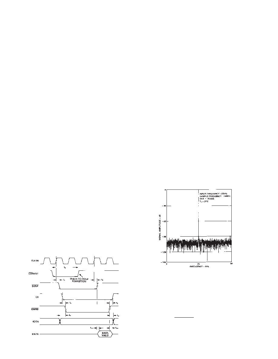
The output spectrum from the ADC is evaluated by applying a
sine-wave signal of very low distortion to the VIN input, which is
sampled at a 100 kHz sampling rate. A Fast Fourier Transform
(FFT) plot is generated from which the SNR data can be ob-
tained. Figure 10 shows a typical 2048 point FFT plot of the
AD7878KN with an input signal of 25 kHz and a sampling
frequency of 100 kHz. The SNR obtained from this graph is
72.6 dB. It should be noted that the harmonics are included in
the SNR calculation.
Figure 10. AD7878 FFT Plot
Effective Number of Bits
The formula given in (1) relates the SNR to the number of bits.
Rewriting the formula, as in (2), it is possible to get a measure of
performance expressed in effective number of bits (N). The
effective number of bits for a device can be calculated directly
from its measured SNR.
N
=
SNR –1.76
6.02
(2)
相关PDF资料 |
PDF描述 |
|---|---|
| IDT72V801L15PFI8 | IC SYNC FIFO 256X9 15NS 64QFP |
| LTC1350ISW | IC TXRX 3.3V EIA/TIA-562 28-SOIC |
| VE-B6F-MW-F4 | CONVERTER MOD DC/DC 72V 100W |
| MS3106R28-11SX | CONN PLUG 22POS STRAIGHT W/SCKT |
| VI-B1Z-MX | CONVERTER MOD DC/DC 2V 30W |
相关代理商/技术参数 |
参数描述 |
|---|---|
| AD7878JP | 制造商:Analog Devices 功能描述:ADC Single SAR 100ksps 12-bit Parallel 28-Pin PLCC 制造商:Rochester Electronics LLC 功能描述:12-BIT ADC IC - Bulk |
| AD7878JPZ | 功能描述:IC ADC 12BIT W/DSP INT 28-PLCC RoHS:是 类别:集成电路 (IC) >> 数据采集 - 模数转换器 系列:- 产品培训模块:Lead (SnPb) Finish for COTS Obsolescence Mitigation Program 标准包装:2,500 系列:- 位数:12 采样率(每秒):3M 数据接口:- 转换器数目:- 功率耗散(最大):- 电压电源:- 工作温度:- 安装类型:表面贴装 封装/外壳:SOT-23-6 供应商设备封装:SOT-23-6 包装:带卷 (TR) 输入数目和类型:- |
| AD7878JPZ-REEL | 功能描述:IC ADC 12BIT W/DSP 28PLCC RoHS:是 类别:集成电路 (IC) >> 数据采集 - 模数转换器 系列:- 标准包装:1 系列:- 位数:14 采样率(每秒):83k 数据接口:串行,并联 转换器数目:1 功率耗散(最大):95mW 电压电源:双 ± 工作温度:0°C ~ 70°C 安装类型:通孔 封装/外壳:28-DIP(0.600",15.24mm) 供应商设备封装:28-PDIP 包装:管件 输入数目和类型:1 个单端,双极 |
| AD7878KN | 制造商:Analog Devices 功能描述:ADC Single SAR 100ksps 12-bit Parallel 28-Pin PDIP W 制造商:Rochester Electronics LLC 功能描述:COMPLETE 12 BIT ADC IC - Bulk |
| AD7878KP | 制造商:Rochester Electronics LLC 功能描述:12-BIT ADC IC - Bulk 制造商:Analog Devices 功能描述: |
发布紧急采购,3分钟左右您将得到回复。