参数资料
| 型号: | AD7886JD |
| 厂商: | Analog Devices Inc |
| 文件页数: | 11/16页 |
| 文件大小: | 0K |
| 描述: | IC ADC 12BIT SAMPLING HS 28-CDIP |
| 标准包装: | 1 |
| 位数: | 12 |
| 采样率(每秒): | 1M |
| 数据接口: | 并联 |
| 转换器数目: | 1 |
| 功率耗散(最大): | 350mW |
| 电压电源: | 双 ± |
| 工作温度: | 0°C ~ 70°C |
| 安装类型: | 通孔 |
| 封装/外壳: | 28-CDIP(0.605",15.37mm) |
| 供应商设备封装: | 28-CDIP |
| 包装: | 管件 |
| 输入数目和类型: | 2 个单端,单极;2 个单端,双极 |
AD7886
–4–
REV. B
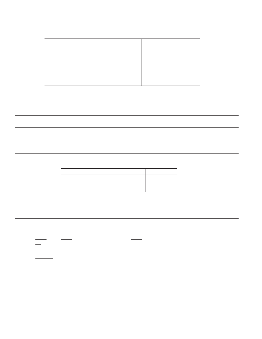
ORDERING GUIDE
Integral
Temperature
SNR
Nonlinearity
Package
Model1, 2
Range
(dBs)
(LSBs)
Option3
AD7886JD
0
°C to +70°C
65
D-28
AD7886KD
0
°C to +70°C67
±2.0
D-28
AD7886JP
0
°C to +70°C
65
P-28A
2
AD7886KP
0
°C to +70°C67
±2.0
P-28A
2
AD7886BD
–40
°C to +85°C67
±2.0
D-28
AD7886TD
–55
°C to +125°C65
±2.0
D-28
NOTES
1Contact your sales office for availability of AD7886BD, AD7886TD and 1 MHz version.
2Analog Devices reserves the right to ship J-Leaded Ceramic Chip Carrier (JLCCC) in lieu of PLCC packages.
3D = Ceramic DIP; P = Plastic Leaded Chip Carrier.
PIN FUNCTION DESCRIPTION
DIP Pin
Number
Mnemonic
Description
Power Supply
10 & 19
VDD
Positive Power Supply, +5 V
± 5%. Both V
DD pins must be tied together.
15 & 24
VSS
Negative Power Supply, –5 V
± 5%. Both V
SS pins must be tied together.
16 & 23
AGND
Analog Ground. Both AGND pins must be tied together.
5
DGND
Digital Ground.
Analog and Reference Inputs
17 & 18
VIN
Analog Inputs, VIN1 and VIN2. The part can be pin strapped for any one of three analog input ranges;
Range
Pin Strap
Signal Input
0 V to 5 V
Connect VIN2 to VIN1
VIN1 & VIN2
0 V to 10 V
Connect VIN2 to GND
VIN1
±5 V
Connect VIN2 to +5 V
VIN1
20
+5REF
+5 V Reference input. This input is used in conjunction with SUM and VREF inputs to scale an external
+5 V reference to –3.5 V, the required reference for the part (see Figure 2).
21
SUM
Summing Point. This input is used in conjunction with +5REF and VREF inputs to scale an external
+5 V reference to –3.5 V, the required reference for the part (see Figure 2).
22
VREF
Voltage Reference Input. The AD7886 is specified with VREF = –3.5 V.
Interface and Control
1–4,
DB7–DB4
Three-state data outputs.
6–9,
DB3–DB0
These outputs are controlled by
CS and RD. DB11 is the Most Significant Bit (MSB).
25–28
DB11–DB8
11
BUSY
BUSY Output indicates converter status. BUSY is low during conversion.
12
CS
Chip Select Input. The device is selected when this input is low.
13
RD
Read Input. This active low signal, in conjunction with
CS, is used to enable the output data three-state
drivers.
14
CONVST
Conversion Start Input. This input is used to start conversion.
相关PDF资料 |
PDF描述 |
|---|---|
| AD7887ARZ-REEL | IC ADC 12BIT 2CHAN SRL 8SOIC |
| AD7888ARZ-REEL | IC ADC 12BIT 8CH SRL 16-SOIC |
| AD7889-1ACBZ-500R7 | IC ADC 12BIT CTRLR TOUCH 12WLCSP |
| AD7892ANZ-2 | IC ADC 12BIT LP 500KSPS 24DIP |
| AD7893BRZ-2REEL7 | IC ADC 12BIT SRL T/H LP 8SOIC |
相关代理商/技术参数 |
参数描述 |
|---|---|
| AD7886JP | 功能描述:IC ADC 12BIT SAMPLING HS 28-PLCC RoHS:否 类别:集成电路 (IC) >> 数据采集 - 模数转换器 系列:- 标准包装:1 系列:- 位数:14 采样率(每秒):83k 数据接口:串行,并联 转换器数目:1 功率耗散(最大):95mW 电压电源:双 ± 工作温度:0°C ~ 70°C 安装类型:通孔 封装/外壳:28-DIP(0.600",15.24mm) 供应商设备封装:28-PDIP 包装:管件 输入数目和类型:1 个单端,双极 |
| AD7886JP-REEL | 功能描述:IC ADC 12BIT SAMPLING HS 28-PLCC RoHS:否 类别:集成电路 (IC) >> 数据采集 - 模数转换器 系列:- 标准包装:1 系列:- 位数:14 采样率(每秒):83k 数据接口:串行,并联 转换器数目:1 功率耗散(最大):95mW 电压电源:双 ± 工作温度:0°C ~ 70°C 安装类型:通孔 封装/外壳:28-DIP(0.600",15.24mm) 供应商设备封装:28-PDIP 包装:管件 输入数目和类型:1 个单端,双极 |
| AD7886KP-REEL | 制造商:Analog Devices 功能描述: |
| AD7887AR | 功能描述:IC ADC 12BIT 2CH SRL 8-SOIC RoHS:否 类别:集成电路 (IC) >> 数据采集 - 模数转换器 系列:- 标准包装:1,000 系列:- 位数:16 采样率(每秒):45k 数据接口:串行 转换器数目:2 功率耗散(最大):315mW 电压电源:模拟和数字 工作温度:0°C ~ 70°C 安装类型:表面贴装 封装/外壳:28-SOIC(0.295",7.50mm 宽) 供应商设备封装:28-SOIC W 包装:带卷 (TR) 输入数目和类型:2 个单端,单极 |
| AD7887ARM | 功能描述:IC ADC 12BIT 2CH SRL 8-MSOP RoHS:否 类别:集成电路 (IC) >> 数据采集 - 模数转换器 系列:- 标准包装:1,000 系列:- 位数:16 采样率(每秒):45k 数据接口:串行 转换器数目:2 功率耗散(最大):315mW 电压电源:模拟和数字 工作温度:0°C ~ 70°C 安装类型:表面贴装 封装/外壳:28-SOIC(0.295",7.50mm 宽) 供应商设备封装:28-SOIC W 包装:带卷 (TR) 输入数目和类型:2 个单端,单极 |
发布紧急采购,3分钟左右您将得到回复。