参数资料
| 型号: | AD7886JD |
| 厂商: | Analog Devices Inc |
| 文件页数: | 13/16页 |
| 文件大小: | 0K |
| 描述: | IC ADC 12BIT SAMPLING HS 28-CDIP |
| 标准包装: | 1 |
| 位数: | 12 |
| 采样率(每秒): | 1M |
| 数据接口: | 并联 |
| 转换器数目: | 1 |
| 功率耗散(最大): | 350mW |
| 电压电源: | 双 ± |
| 工作温度: | 0°C ~ 70°C |
| 安装类型: | 通孔 |
| 封装/外壳: | 28-CDIP(0.605",15.37mm) |
| 供应商设备封装: | 28-CDIP |
| 包装: | 管件 |
| 输入数目和类型: | 2 个单端,单极;2 个单端,双极 |
AD7886
–6–
REV. B
this amplifier typically by 20 MHz which is much greater than
the Nyquist limit of the ADC; as a result, it can be used for
undersampling applications. The track-and-hold amplifier ac-
quires the input signal to 12-bit accuracy in less than 333 ns.
The overall throughput time is equal to the conversion time
plus the track/ hold amplifier acquisition time, which is 1.333
s
for the AD7886.
The operation of the track/hold amplifier is essentially transpar-
ent to the user. The track-to-hold transition occurs at the start
of conversion on the falling edge of
CONVST. The conversion
procedure does not start until the rising edge of
CONVST. The
width of the
CONVST pulse low time determines the track-to
hold settling time. The track/hold reverts back to the track
mode at the end of conversion when
BUSY has returned high.
+
–
TO
COMPARATORS
VIN1
VIN2
0 TO 5V
0 TO 5V ANALOG INPUT RANGE
3.5k
10k
0 TO 10V ANALOG INPUT RANGE
+
–
TO
COMPARATORS
VIN1
VIN2
0 TO 10V
3.5k
10k
+5V
±5V ANALOG INPUT RANGE
±5V
+
–
TO
COMPARATORS
VIN1
VIN2
3.5k
10k
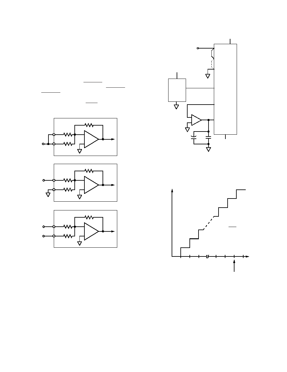
Figure 3. Analog Input Range Configurations
ANALOG INPUT RANGES
The AD7886 has three user selectable analog input ranges: 0 V
to 5 V, 0 V to 10 V and
±5 V. Figure 3 shows how to configure
the two analog inputs (VIN1 and VIN2) for these ranges.
UNIPOLAR OPERATION
Figure 4 shows a typical unipolar circuit for the AD7886. The
ideal input/output characteristic is shown in Figure 5. The
designed code transitions occur on integer multiples of 1 LSB.
The output code is natural binary with 1 LSB = FS/4096. FS is
either +5 V or +10 V, depending on how the analog inputs are
configured.
AD7886*
SUM
+
–
AD586
V
OUT
+V
IN
GND
+V
C1
10
F
C2
0.1
F
AD707
VIN1
VIN2**
AGND
V
SS
V
DD
AIN
0 TO 5V
OR
0 TO 10V
5V
+
5REF
+
5V
+
V
REF
3.5V
–
5V
–
*ADDITIONAL PINS OMITTED FOR CLARITY
**0 TO 5V RANGE: CONNECT VIN2 TO VIN1
0 TO 10V RANGE: CONNECT VIN2 TO AGND
Figure 4. Unipolar Operation
00...000
00...001
00...010
00...011
11...111
11...110
11...101
11...100
123
FS
OUTPUT
CODE
VIN, INPUT VOLTAGE (LSBS)
FS – 1LSB
1LSB =
4096
FS
Figure 5. Ideal Input/Output Transfer Characteristic for
Unipolar Operation
相关PDF资料 |
PDF描述 |
|---|---|
| AD7887ARZ-REEL | IC ADC 12BIT 2CHAN SRL 8SOIC |
| AD7888ARZ-REEL | IC ADC 12BIT 8CH SRL 16-SOIC |
| AD7889-1ACBZ-500R7 | IC ADC 12BIT CTRLR TOUCH 12WLCSP |
| AD7892ANZ-2 | IC ADC 12BIT LP 500KSPS 24DIP |
| AD7893BRZ-2REEL7 | IC ADC 12BIT SRL T/H LP 8SOIC |
相关代理商/技术参数 |
参数描述 |
|---|---|
| AD7886JP | 功能描述:IC ADC 12BIT SAMPLING HS 28-PLCC RoHS:否 类别:集成电路 (IC) >> 数据采集 - 模数转换器 系列:- 标准包装:1 系列:- 位数:14 采样率(每秒):83k 数据接口:串行,并联 转换器数目:1 功率耗散(最大):95mW 电压电源:双 ± 工作温度:0°C ~ 70°C 安装类型:通孔 封装/外壳:28-DIP(0.600",15.24mm) 供应商设备封装:28-PDIP 包装:管件 输入数目和类型:1 个单端,双极 |
| AD7886JP-REEL | 功能描述:IC ADC 12BIT SAMPLING HS 28-PLCC RoHS:否 类别:集成电路 (IC) >> 数据采集 - 模数转换器 系列:- 标准包装:1 系列:- 位数:14 采样率(每秒):83k 数据接口:串行,并联 转换器数目:1 功率耗散(最大):95mW 电压电源:双 ± 工作温度:0°C ~ 70°C 安装类型:通孔 封装/外壳:28-DIP(0.600",15.24mm) 供应商设备封装:28-PDIP 包装:管件 输入数目和类型:1 个单端,双极 |
| AD7886KP-REEL | 制造商:Analog Devices 功能描述: |
| AD7887AR | 功能描述:IC ADC 12BIT 2CH SRL 8-SOIC RoHS:否 类别:集成电路 (IC) >> 数据采集 - 模数转换器 系列:- 标准包装:1,000 系列:- 位数:16 采样率(每秒):45k 数据接口:串行 转换器数目:2 功率耗散(最大):315mW 电压电源:模拟和数字 工作温度:0°C ~ 70°C 安装类型:表面贴装 封装/外壳:28-SOIC(0.295",7.50mm 宽) 供应商设备封装:28-SOIC W 包装:带卷 (TR) 输入数目和类型:2 个单端,单极 |
| AD7887ARM | 功能描述:IC ADC 12BIT 2CH SRL 8-MSOP RoHS:否 类别:集成电路 (IC) >> 数据采集 - 模数转换器 系列:- 标准包装:1,000 系列:- 位数:16 采样率(每秒):45k 数据接口:串行 转换器数目:2 功率耗散(最大):315mW 电压电源:模拟和数字 工作温度:0°C ~ 70°C 安装类型:表面贴装 封装/外壳:28-SOIC(0.295",7.50mm 宽) 供应商设备封装:28-SOIC W 包装:带卷 (TR) 输入数目和类型:2 个单端,单极 |
发布紧急采购,3分钟左右您将得到回复。