- 您现在的位置:买卖IC网 > PDF目录10118 > AD7892ANZ-3 (Analog Devices Inc)IC ADC 12BIT LP 600KSPS 24DIP PDF资料下载
参数资料
| 型号: | AD7892ANZ-3 |
| 厂商: | Analog Devices Inc |
| 文件页数: | 12/14页 |
| 文件大小: | 0K |
| 描述: | IC ADC 12BIT LP 600KSPS 24DIP |
| 标准包装: | 15 |
| 位数: | 12 |
| 采样率(每秒): | 600k |
| 数据接口: | 串行,并联 |
| 转换器数目: | 1 |
| 功率耗散(最大): | 90mW |
| 电压电源: | 单电源 |
| 工作温度: | -40°C ~ 85°C |
| 安装类型: | 通孔 |
| 封装/外壳: | 24-DIP(0.300",7.62mm) |
| 供应商设备封装: | 24-PDIP |
| 包装: | 管件 |
| 输入数目和类型: | 2 个单端,双极 |
AD7892
REV. C
–7–
Pin
No.
Mnemonic
Description
16
DB4/SCLK
Data Bit 4/Serial Clock. When the device is in its parallel mode, this pin is Data Bit 4, a three-state
TTL-compatible output. When the device is in its serial mode, this becomes the serial clock pin,
SCLK. SCLK is an input and an external serial clock must be provided at this pin to obtain serial
data from the AD7892. Serial data is clocked out from the output shift register on the rising edges
of SCLK after
RFS goes low.
17
DB3/
RFS
Data Bit 3/Receive Frame Synchronization. When the device is in its parallel mode, this pin is Data
Bit 3, a three-state TTL-compatible output. When the device is in its serial mode, this becomes the
receive frame synchronization input with
RFS provided externally to obtain serial data from the
AD7892.
18
DB2
Data Bit 2. Three-state TTL-compatible output. This output should be left unconnected when the
device is in its serial mode.
19
DB1
Data Bit 1. Three-state TTL-compatible output. This output should be left unconnected when the
device is in its serial mode.
20
DB0
Data Bit 0 (LSB). Three-state TTL-compatible output. Output coding is two’s complement for
AD7892-1 and AD7892-3 and straight (natural) binary for AD7892-2. This output should be left
unconnected when the device is in its serial mode.
21
RD
Read. Active low logic input which is used in conjunction with
CS low to enable the data outputs.
22
CS
Chip Select. Active low logic input which is used in conjunction with
RD to enable the data outputs.
23
EOC
End-of-Conversion. Active low logic output indicating converter status. The end of conversion is
signified by a low going pulse on this line. The duration of this
EOC pulse is nominally 100 ns.
24
CONVST
Convert Start. Logic Input. A low-to-high transition on this input puts the track/hold into its hold
mode and starts conversion.
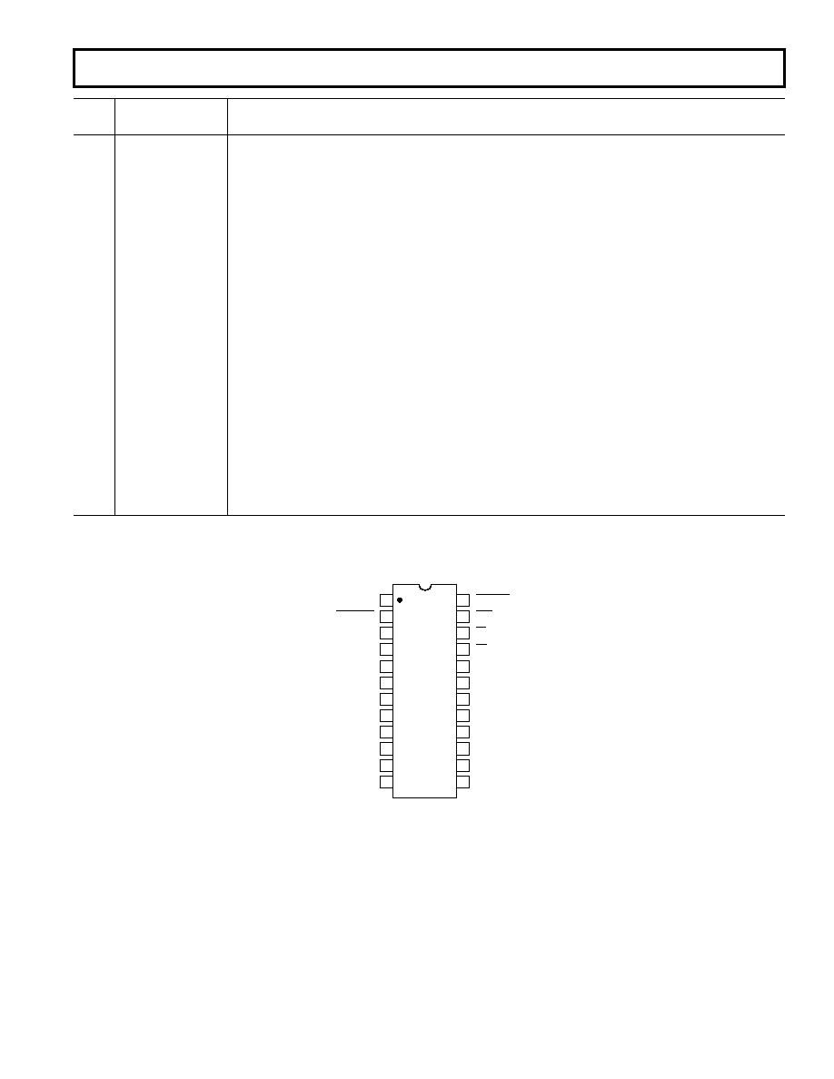
PIN CONFIGURATION
DIP and SOIC
VDD
REF OUT/REF IN
AGND
MODE
DB0 (LSB)
DB1
DB2
VIN2
VIN1
DB11/LOW
DB3/
RFS
DB10/LOW
DB4/SCLK
DB9
DB5/SDATA
DB8
DGND
DB7
DB6
14
1
2
24
23
5
6
7
20
19
18
3
4
22
21
817
916
10
15
11
TOP VIEW
(Not to Scale)
11
12
13
AD7892
STANDBY
CONVST
EOC
CS
RD
相关PDF资料 |
PDF描述 |
|---|---|
| MS27656T19B35P | CONN RCPT 66POS WALL MNT W/PINS |
| MS27656T21B39PA | CONN RCPT 39POS WALL MNT W/PINS |
| MS3106R12S-3SZ | CONN PLUG 2POS STRAIGHT W/SCKT |
| D38999/24WC98SD | CONN RCPT 10POS JAM NUT W/SCKT |
| VI-2NP-MX-F3 | CONVERTER MOD DC/DC 13.8V 75W |
相关代理商/技术参数 |
参数描述 |
|---|---|
| AD7892AR-1 | 功能描述:IC ADC 12BIT LP 500KSPS 24-SOIC RoHS:否 类别:集成电路 (IC) >> 数据采集 - 模数转换器 系列:- 标准包装:1 系列:- 位数:14 采样率(每秒):83k 数据接口:串行,并联 转换器数目:1 功率耗散(最大):95mW 电压电源:双 ± 工作温度:0°C ~ 70°C 安装类型:通孔 封装/外壳:28-DIP(0.600",15.24mm) 供应商设备封装:28-PDIP 包装:管件 输入数目和类型:1 个单端,双极 |
| AD7892AR-1REEL | 功能描述:IC ADC 12BIT LP 500KSPS 24-SOIC RoHS:否 类别:集成电路 (IC) >> 数据采集 - 模数转换器 系列:- 标准包装:1,000 系列:- 位数:12 采样率(每秒):300k 数据接口:并联 转换器数目:1 功率耗散(最大):75mW 电压电源:单电源 工作温度:0°C ~ 70°C 安装类型:表面贴装 封装/外壳:24-SOIC(0.295",7.50mm 宽) 供应商设备封装:24-SOIC 包装:带卷 (TR) 输入数目和类型:1 个单端,单极;1 个单端,双极 |
| AD7892AR-1Z | 制造商:Analog Devices 功能描述:IC, 12BIT ADC 600KSPS, SMD, WSOIC24 |
| AD7892AR-2 | 功能描述:IC ADC 12BIT LP 500KSPS 24-SOIC RoHS:否 类别:集成电路 (IC) >> 数据采集 - 模数转换器 系列:- 标准包装:1 系列:- 位数:14 采样率(每秒):83k 数据接口:串行,并联 转换器数目:1 功率耗散(最大):95mW 电压电源:双 ± 工作温度:0°C ~ 70°C 安装类型:通孔 封装/外壳:28-DIP(0.600",15.24mm) 供应商设备封装:28-PDIP 包装:管件 输入数目和类型:1 个单端,双极 |
| AD7892AR-2REEL | 制造商:Analog Devices 功能描述:ADC Single SAR 500ksps 12-bit Parallel/Serial 24-Pin SOIC W T/R 制造商:Rochester Electronics LLC 功能描述:12-BIT 500 KSPS PARALLEL ADC I.C. - Tape and Reel |
发布紧急采购,3分钟左右您将得到回复。