- 您现在的位置:买卖IC网 > PDF目录10118 > AD7892ANZ-3 (Analog Devices Inc)IC ADC 12BIT LP 600KSPS 24DIP PDF资料下载
参数资料
| 型号: | AD7892ANZ-3 |
| 厂商: | Analog Devices Inc |
| 文件页数: | 14/14页 |
| 文件大小: | 0K |
| 描述: | IC ADC 12BIT LP 600KSPS 24DIP |
| 标准包装: | 15 |
| 位数: | 12 |
| 采样率(每秒): | 600k |
| 数据接口: | 串行,并联 |
| 转换器数目: | 1 |
| 功率耗散(最大): | 90mW |
| 电压电源: | 单电源 |
| 工作温度: | -40°C ~ 85°C |
| 安装类型: | 通孔 |
| 封装/外壳: | 24-DIP(0.300",7.62mm) |
| 供应商设备封装: | 24-PDIP |
| 包装: | 管件 |
| 输入数目和类型: | 2 个单端,双极 |
AD7892
REV. C
–9–
CIRCUIT DESCRIPTION
The AD7892 is a fast, 12-bit single supply A/D converter. It
provides the user with signal scaling, track/hold, reference, A/D
converter and versatile interface logic functions on a single chip.
The signal scaling on the AD7892-1 allows the part to handle
either
±5 V or ±10 V input signals while operating from a single
+5 V supply. The AD7892-2 handles a 0 V to +2.5 V analog
input range, while signal scaling on the AD7892-3 allows it to
handle
±2.5 V input signals when operating from a single supply.
The part requires a +2.5 V reference which can be provided from
the part’s own internal reference or from an external reference
source.
Conversion is initiated on the AD7892 by pulsing the
CONVST
input. On the rising edge of
CONVST, the track/hold goes
from track mode to hold mode and the conversion sequence is
started. At the end of conversion (falling edge of
EOC), the
track/hold returns to tracking mode and the acquisition time
begins. Conversion time for the part is 1.47
s (AD7892-3) and
the track/hold acquisition time is 200 ns (AD7892-3). This allows
the AD7892-3 to operate at throughput rates up to 600 kSPS.
The AD7892-1 and AD7892-2 are specified with a 1.6
s con-
version and 400 ns acquisition time allowing a throughput rate
of 500 kSPS.
Track/Hold Section
The track/hold amplifier on the AD7892 allows the ADC to
accurately convert an input sine wave of full-scale amplitude to
12-bit accuracy. The input bandwidth of the track/hold is greater
than the Nyquist rate of the ADC even when the ADC is oper-
ated at its maximum throughput rate of 600 kHz (i.e., the track/
hold can handle input frequencies in excess of 300 kHz).
The track/hold amplifier acquires an input signal to 12-bit accu-
racy in less than 200 ns. The operation of the track/hold is
essentially transparent to the user. The track/hold amplifier
goes from its tracking mode to its hold mode on the rising edge
of
CONVST. The aperture time for the track/hold (i.e., the
delay time between the external
CONVST signal and the track/
hold actually going into hold) is typically 15 ns. At the end of
conversion, the part returns to its tracking mode. The acquisi-
tion time of the track/hold amplifier begins at this point.
Reference Section
The AD7892 contains a single reference pin, labelled REF OUT/
REF IN, which either provides access to the part’s own +2.5 V
reference or to which an external +2.5 V reference can be con-
nected to provide the reference source for the part. The part is
specified with a +2.5 V reference voltage. Errors in the refer-
ence source will result in gain errors in the AD7892’s transfer
function and will add to the specified full-scale errors on the
part. On the AD7892-1 and AD7892-3, it will also result in an
offset error injected in the attenuator stage.
The AD7892 contains an on-chip +2.5 V reference. To use this
reference as the reference source for the AD7892, simply con-
nect a 0.1
F disc ceramic capacitor from the REF OUT/
REF IN pin to AGND. The voltage that appears at this pin is
internally buffered before being applied to the ADC. If this
reference is required for use external to the AD7892, it should
be buffered as the part has a FET switch in series with the refer-
ence output resulting in a source impedance for this output of
5.5 k
nominal. The tolerance on the internal reference is
±10 mV at 25°C with a typical temperature coefficient of
25 ppm/
°C and a maximum error over temperature of ±25 mV.
If the application requires a reference with a tighter tolerance or
the AD7892 needs to be used with a system reference, then the
user has the option of connecting an external reference to this
REF OUT/REF IN pin. The external reference will effectively
overdrive the internal reference and thus provide the reference
source for the ADC. The reference input is buffered before
being applied to the ADC with the maximum input current is
±100 A. Suitable reference sources for the AD7892 include the
AD680, AD780 and REF43 precision +2.5 V references.
INTERFACING
The part provides two interface options, a 12-bit parallel inter-
face and a three-wire serial interface. The required interface
mode is selected via the MODE pin. The two interface modes
are discussed in the following sections.
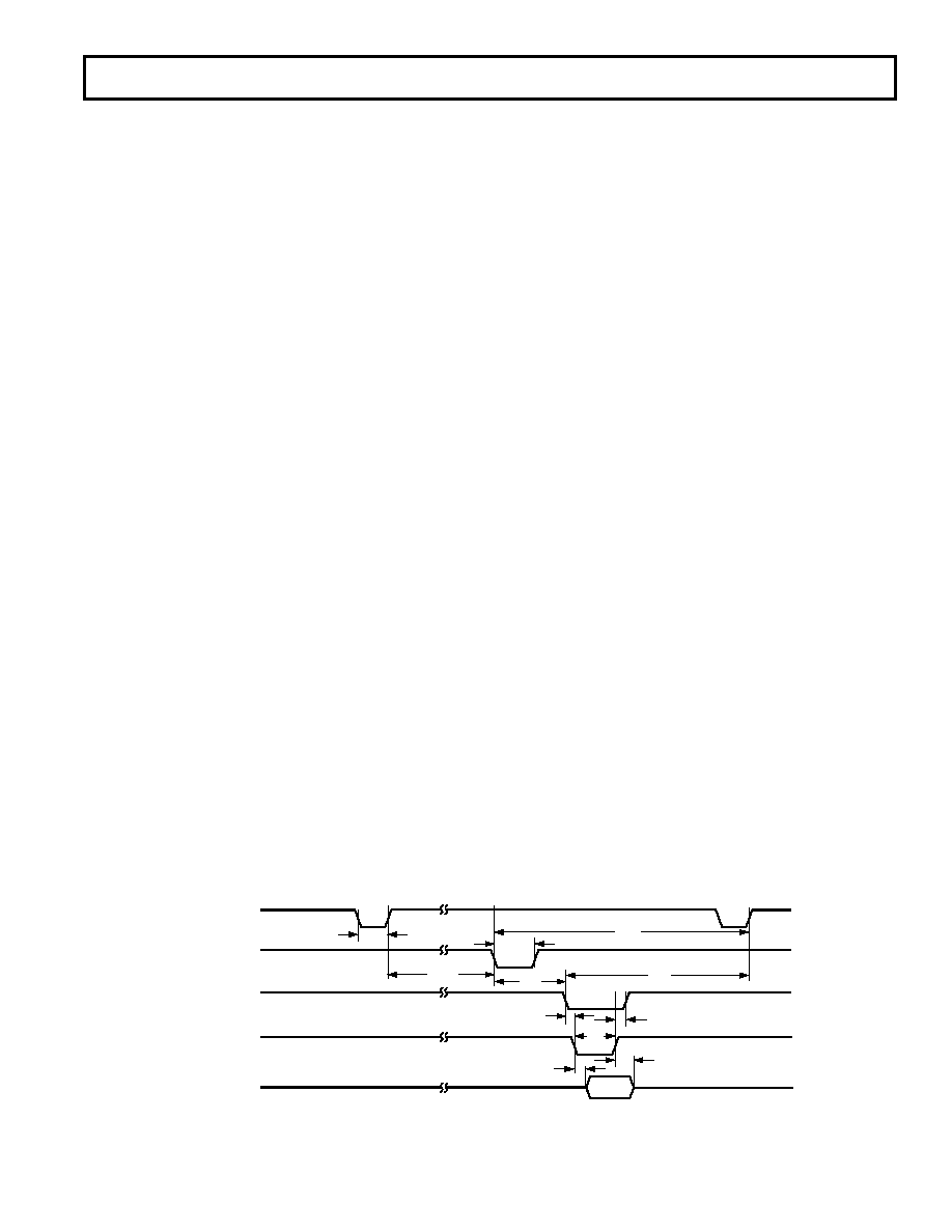
Parallel Interface Mode
The parallel interface mode is selected by tying the MODE
input to a logic high. Figure 2 shows a timing diagram illustrat-
ing the operational sequence of the AD7892. The on-chip
track/hold goes into hold mode, and conversion is initiated on
the rising edge of the
CONVST signal. When conversion is
complete, the end of conversion line (
EOC) pulses low to indi-
cate that new data is available in the AD7892’s output register.
This
EOC line can be used to drive an edge-triggered interrupt
of a microprocessor. The falling edge of the
RD signal should
occur 200 ns prior to the next rising edge of
CONVST. CS and
RD going low accesses the 12-bit conversion result. In systems
where the part is interfaced to a gate array or ASIC, this
EOC
VALID
DATA
tCONV
t8
t5
t4
t7
t6
t2
t1
THREE-STATE
CONVST (I)
EOC (O)
CS (I)
RD (I)
DB0–DB11 (O)
NOTE:
I = INPUT; O = OUTPUT
tACQ
t3
t9
THREE-STATE
Figure 2. Parallel Mode Timing Diagram
相关PDF资料 |
PDF描述 |
|---|---|
| MS27656T19B35P | CONN RCPT 66POS WALL MNT W/PINS |
| MS27656T21B39PA | CONN RCPT 39POS WALL MNT W/PINS |
| MS3106R12S-3SZ | CONN PLUG 2POS STRAIGHT W/SCKT |
| D38999/24WC98SD | CONN RCPT 10POS JAM NUT W/SCKT |
| VI-2NP-MX-F3 | CONVERTER MOD DC/DC 13.8V 75W |
相关代理商/技术参数 |
参数描述 |
|---|---|
| AD7892AR-1 | 功能描述:IC ADC 12BIT LP 500KSPS 24-SOIC RoHS:否 类别:集成电路 (IC) >> 数据采集 - 模数转换器 系列:- 标准包装:1 系列:- 位数:14 采样率(每秒):83k 数据接口:串行,并联 转换器数目:1 功率耗散(最大):95mW 电压电源:双 ± 工作温度:0°C ~ 70°C 安装类型:通孔 封装/外壳:28-DIP(0.600",15.24mm) 供应商设备封装:28-PDIP 包装:管件 输入数目和类型:1 个单端,双极 |
| AD7892AR-1REEL | 功能描述:IC ADC 12BIT LP 500KSPS 24-SOIC RoHS:否 类别:集成电路 (IC) >> 数据采集 - 模数转换器 系列:- 标准包装:1,000 系列:- 位数:12 采样率(每秒):300k 数据接口:并联 转换器数目:1 功率耗散(最大):75mW 电压电源:单电源 工作温度:0°C ~ 70°C 安装类型:表面贴装 封装/外壳:24-SOIC(0.295",7.50mm 宽) 供应商设备封装:24-SOIC 包装:带卷 (TR) 输入数目和类型:1 个单端,单极;1 个单端,双极 |
| AD7892AR-1Z | 制造商:Analog Devices 功能描述:IC, 12BIT ADC 600KSPS, SMD, WSOIC24 |
| AD7892AR-2 | 功能描述:IC ADC 12BIT LP 500KSPS 24-SOIC RoHS:否 类别:集成电路 (IC) >> 数据采集 - 模数转换器 系列:- 标准包装:1 系列:- 位数:14 采样率(每秒):83k 数据接口:串行,并联 转换器数目:1 功率耗散(最大):95mW 电压电源:双 ± 工作温度:0°C ~ 70°C 安装类型:通孔 封装/外壳:28-DIP(0.600",15.24mm) 供应商设备封装:28-PDIP 包装:管件 输入数目和类型:1 个单端,双极 |
| AD7892AR-2REEL | 制造商:Analog Devices 功能描述:ADC Single SAR 500ksps 12-bit Parallel/Serial 24-Pin SOIC W T/R 制造商:Rochester Electronics LLC 功能描述:12-BIT 500 KSPS PARALLEL ADC I.C. - Tape and Reel |
发布紧急采购,3分钟左右您将得到回复。