- 您现在的位置:买卖IC网 > PDF目录10144 > AD7893AN-5 (Analog Devices Inc)IC ADC 12BIT SRL T/H LP 8-DIP PDF资料下载
参数资料
| 型号: | AD7893AN-5 |
| 厂商: | Analog Devices Inc |
| 文件页数: | 12/12页 |
| 文件大小: | 0K |
| 描述: | IC ADC 12BIT SRL T/H LP 8-DIP |
| 标准包装: | 1 |
| 位数: | 12 |
| 采样率(每秒): | 117k |
| 数据接口: | 串行 |
| 转换器数目: | 1 |
| 功率耗散(最大): | 45mW |
| 电压电源: | 单电源 |
| 工作温度: | -40°C ~ 85°C |
| 安装类型: | 通孔 |
| 封装/外壳: | 8-DIP(0.300",7.62mm) |
| 供应商设备封装: | 8-PDIP |
| 包装: | 管件 |
| 输入数目和类型: | 1 个单端,单极 |
AD7893
–9–
REV. E
The AD7893 counts the serial clock edges to know which bit
from the output register should be placed on the SDATA out-
put. To ensure that the part does not lose synchronization, the
serial clock counter is reset on the falling edge of the CONVST
input, provided the SCLR line is low. The user should ensure
that a falling edge on the CONVST input does not occur while
a serial data read operation is in progress.
MICROPROCESSOR/MICROCONTROLLER INTERFACE
The AD7893 provides a two-wire serial interface that can be
used for connection to the serial ports of DSP processors and
microcontrollers. Figures 6 through 9 show the AD7893 inter-
faced to a number of different microcontrollers and DSP pro-
cessors. The AD7893 accepts an external serial clock and, as a
result, in all interfaces shown here, the processor/controller is
configured as the master, providing the serial clock with the
AD7893 configured as the slave in the system.
AD7893-8051 Interface
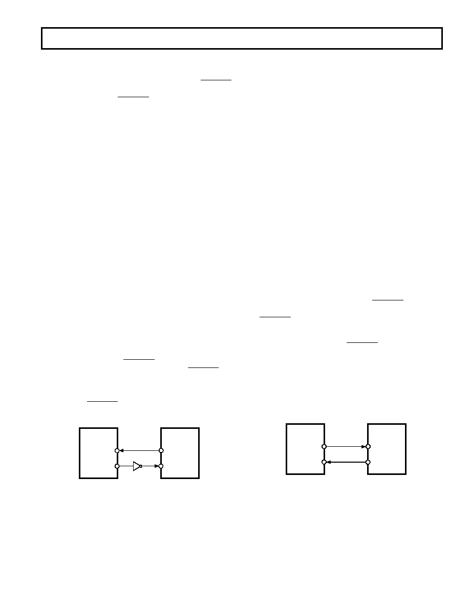
Figure 6 shows an interface between the AD7893 and the
8XC51 microcontroller. The 8XC51 is configured for its Mode
0 serial interface mode. The diagram shows the simplest form of
the interface where the AD7893 is the only part connected to
the serial port of the 8XC51 and, therefore, no decoding of the
serial read operations is required. It also makes no provisions for
monitoring when conversion is complete on the AD7893.
Either of these two tasks can readily be accomplished with minor
modifications to the interface. To chip select the AD7893 in
systems where more than one device is connected to the 8XC51’s
serial port, a port bit configured as an output from one of the
8XC51’s parallel ports can be used to gate on or off the serial
clock to the AD7893. A simple AND function on this port bit
and the serial clock from the 8XC51 will provide this function.
The port bit should be high to select the AD7893 and low when
it is not selected.
To monitor the conversion time on the AD7893, a scheme such
as previously outlined with CONVST can be used. This can be
implemented in two ways. One is to connect the CONVST line
to another parallel port bit that is configured as an input. This
port bit can then be polled to determine when conversion is
complete. An alternative is to use an interrupt driven system, in
which case the CONVST line should be connected to the INT1
input of the 8XC51.
The serial clock rate from the 8XC51 is limited to significantly
less than the allowable input serial clock frequency with which
the AD7893 can operate. As a result, the time to read data from
the part will actually be longer than the conversion time of the
part. This means that the AD7893 cannot run at its maximum
throughput rate when used with the 8XC51.
AD7893-68HC11 Interface
An interface circuit between the AD7893 and the 68HC11
microcontroller is shown in Figure 7. For the interface shown,
the 68HC11 SPI port is used, and the 68HC11 is configured in
its single-chip mode. The 68HC11 is configured in the master
mode with its CPOL bit set to a logic zero and its CPHA bit set
to a logic one. As with the previous interface, the diagram shows
the simplest form of the interface where the AD7893 is the only
part connected to the serial port of the 68HC11 and, therefore,
no decoding of the serial read operations is required. It also
makes no provisions for monitoring when conversion is com-
plete on the AD7893.
Once again, either of these two tasks can readily be accom-
plished with minor modifications to the interface. To chip select
the AD7893 in systems where more than one device is con-
nected to the 68HC11’s serial port, a port bit, configured as an
output from one of the 68HC11’s parallel ports, can be used to
gate on or off the serial clock to the AD7893. A simple AND
function on this port bit and the serial clock from the 68HC11
will provide this function. The port bit should be high to select
the AD7893 and low when it is not selected.
To monitor the conversion time on the AD7893, a scheme such
as outlined in the previous interface with CONVST can be
used. This can be implemented in two ways. One is to connect
the CONVST line to another parallel port bit that is configured
as an input. This port bit can then be polled to determine when
conversion is complete. An alternative is to use an interrupt
driven system, in which case the CONVST line should be con-
nected to the IRQ input of the 68HC11.
The serial clock rate from the 68HC11 is limited to significantly
less than the allowable input serial clock frequency with which
the AD7893 can operate. As a result, the time to read data from
the part will actually be longer than the conversion time of the
part. This means that the AD7893 cannot run at its maximum
throughput rate when used with the 68HC11.
AD7893
SDATA
SCLK
8XC51
P3.0
P3.1
Figure 6. AD7893 to 8XC51 Interface
AD7893
SDATA
SCLK
68HC11
SCK
MISO
Figure 7. AD7893 to 68HC11 Interface
相关PDF资料 |
PDF描述 |
|---|---|
| LTC1481IS8 | IC TXRX RS485 LOPWR W/SHTDN8SOIC |
| VE-2NV-MX-F1 | CONVERTER MOD DC/DC 5.8V 75W |
| MS3102E22-12SX | CONN RCPT 5POS BOX MNT W/SCKT |
| LT1785IN8 | IC TXRX RS485/RS422 60V 8-DIP |
| IDT7202LA35J8 | IC FIFO ASYNCH 1KX9 35NS 32PLCC |
相关代理商/技术参数 |
参数描述 |
|---|---|
| AD7893ANZ-10 | 功能描述:IC ADC 12BIT SRL T/H LP 8DIP RoHS:是 类别:集成电路 (IC) >> 数据采集 - 模数转换器 系列:- 标准包装:1 系列:- 位数:14 采样率(每秒):83k 数据接口:串行,并联 转换器数目:1 功率耗散(最大):95mW 电压电源:双 ± 工作温度:0°C ~ 70°C 安装类型:通孔 封装/外壳:28-DIP(0.600",15.24mm) 供应商设备封装:28-PDIP 包装:管件 输入数目和类型:1 个单端,双极 |
| AD7893ANZ-2 | 功能描述:IC ADC 12BIT SRL T/H LP 8-DIP RoHS:是 类别:集成电路 (IC) >> 数据采集 - 模数转换器 系列:- 标准包装:1 系列:microPOWER™ 位数:8 采样率(每秒):1M 数据接口:串行,SPI? 转换器数目:1 功率耗散(最大):- 电压电源:模拟和数字 工作温度:-40°C ~ 125°C 安装类型:表面贴装 封装/外壳:24-VFQFN 裸露焊盘 供应商设备封装:24-VQFN 裸露焊盘(4x4) 包装:Digi-Reel® 输入数目和类型:8 个单端,单极 产品目录页面:892 (CN2011-ZH PDF) 其它名称:296-25851-6 |
| AD7893ANZ-5 | 功能描述:IC ADC 12BIT SRL T/H LP 8DIP RoHS:是 类别:集成电路 (IC) >> 数据采集 - 模数转换器 系列:- 其它有关文件:TSA1204 View All Specifications 标准包装:1 系列:- 位数:12 采样率(每秒):20M 数据接口:并联 转换器数目:2 功率耗散(最大):155mW 电压电源:模拟和数字 工作温度:-40°C ~ 85°C 安装类型:表面贴装 封装/外壳:48-TQFP 供应商设备封装:48-TQFP(7x7) 包装:Digi-Reel® 输入数目和类型:4 个单端,单极;2 个差分,单极 产品目录页面:1156 (CN2011-ZH PDF) 其它名称:497-5435-6 |
| AD7893AR-10 | 功能描述:IC ADC 12BIT SRL T/H LP 8-SOIC RoHS:否 类别:集成电路 (IC) >> 数据采集 - 模数转换器 系列:- 标准包装:1,000 系列:- 位数:12 采样率(每秒):300k 数据接口:并联 转换器数目:1 功率耗散(最大):75mW 电压电源:单电源 工作温度:0°C ~ 70°C 安装类型:表面贴装 封装/外壳:24-SOIC(0.295",7.50mm 宽) 供应商设备封装:24-SOIC 包装:带卷 (TR) 输入数目和类型:1 个单端,单极;1 个单端,双极 |
| AD7893AR-10REEL | 功能描述:IC ADC 12BIT SRL T/H LP 8-SOIC RoHS:否 类别:集成电路 (IC) >> 数据采集 - 模数转换器 系列:- 标准包装:1,000 系列:- 位数:12 采样率(每秒):300k 数据接口:并联 转换器数目:1 功率耗散(最大):75mW 电压电源:单电源 工作温度:0°C ~ 70°C 安装类型:表面贴装 封装/外壳:24-SOIC(0.295",7.50mm 宽) 供应商设备封装:24-SOIC 包装:带卷 (TR) 输入数目和类型:1 个单端,单极;1 个单端,双极 |
发布紧急采购,3分钟左右您将得到回复。