- 您现在的位置:买卖IC网 > PDF目录10144 > AD7893AN-5 (Analog Devices Inc)IC ADC 12BIT SRL T/H LP 8-DIP PDF资料下载
参数资料
| 型号: | AD7893AN-5 |
| 厂商: | Analog Devices Inc |
| 文件页数: | 6/12页 |
| 文件大小: | 0K |
| 描述: | IC ADC 12BIT SRL T/H LP 8-DIP |
| 标准包装: | 1 |
| 位数: | 12 |
| 采样率(每秒): | 117k |
| 数据接口: | 串行 |
| 转换器数目: | 1 |
| 功率耗散(最大): | 45mW |
| 电压电源: | 单电源 |
| 工作温度: | -40°C ~ 85°C |
| 安装类型: | 通孔 |
| 封装/外壳: | 8-DIP(0.300",7.62mm) |
| 供应商设备封装: | 8-PDIP |
| 包装: | 管件 |
| 输入数目和类型: | 1 个单端,单极 |
AD7893
–3–
REV. E
TIMING CHARACTERISTICS
1, 2
A, B
S
Parameter
Versions
Version
Units
Test Conditions/Comments
t1
50
ns min
CONVST
Pulse Width
t2
60
70
ns min
SCLK High Pulse Width
t3
30
40
ns min
SCLK Low Pulse Width
t4
3
50
60
ns max
SCLK Rising Edge to Data Valid Delay
t5
4
10
ns min
Bus Relinquish Time after Falling Edge of SCLK
100
ns max
NOTES
1 Sample tested at +25
°C to ensure compliance. All input signals are measured with tr = tf = 1 ns (10% to 90% of +5 V) and timed from a voltage level of +1.6 V.
2 See Figure 5.
3 Measured with the load circuit of Figure 1 and defined as the time required for an output to cross 0.8 V or 2.4 V.
4 Derived from the measured time taken by the data outputs to change 0.5 V when loaded with the circuit of Figure 1. The measured number is then extrapolated back
to remove the effects of charging or discharging the 50 pF capacitor. This means that the time, t 5, quoted in the timing characteristics is the true bus relinquish time
of the part and, as such, is independent of external bus loading capacitances.
(VDD = +5 V, AGND = DGND = 0 V, REF IN = +2.5 V)
ABSOLUTE MAXIMUM RATINGS*
(TA = +25°C unless otherwise noted)
VDD to AGND . . . . . . . . . . . . . . . . . . . . . . . . . –0.3 V to +7 V
VDD to DGND . . . . . . . . . . . . . . . . . . . . . . . . . –0.3 V to +7 V
Analog Input Voltage to AGND
AD7893-10, AD7893-5 . . . . . . . . . . . . . . . . . . . . . . .
±17 V
AD7893-2, AD7893-3 . . . . . . . . . . . . . . . . . . . –5 V, +10 V
Reference Input Voltage to AGND . . . –0.3 V to VDD + 0.3 V
Digital Input Voltage to DGND . . . . . –0.3 V to VDD + 0.3 V
Digital Output Voltage to DGND . . . . –0.3 V to VDD + 0.3 V
Operating Temperature Range
Commercial (A, B Versions) . . . . . . . . . . . –40
°C to +85°C
Extended (S Version) . . . . . . . . . . . . . . . . –55
°C to +125°C
Storage Temperature Range . . . . . . . . . . . . –65
°C to +150°C
Junction Temperature . . . . . . . . . . . . . . . . . . . . . . . . . +150
°C
Plastic DIP Package, Power Dissipation . . . . . . . . . . 450 mW
θ
JA Thermal Impedance
. . . . . . . . . . . . . . . . . . . . . 130
°C/W
Lead Temperature (Soldering, 10 sec) . . . . . . . . . . . +260
°C
Cerdip Package, Power Dissipation . . . . . . . . . . . . . . 450 mW
θ
JA Thermal Impedance
. . . . . . . . . . . . . . . . . . . . . 125
°C/W
Lead Temperature (Soldering, 10 sec) . . . . . . . . . . . +300
°C
SOIC Package, Power Dissipation . . . . . . . . . . . . . . . 450 mW
θ
JA Thermal Impedance
. . . . . . . . . . . . . . . . . . . . . 170
°C/W
Lead Temperature, Soldering
Vapor Phase (60 sec) . . . . . . . . . . . . . . . . . . . . . . +215
°C
Infrared (15 sec) . . . . . . . . . . . . . . . . . . . . . . . . . . +220
°C
*Stresses above those listed under “Absolute Maximum Ratings” may cause
permanent damage to the device. This is a stress rating only; functional operation
of the device at these or any other conditions above those listed in the operational
sections of this specification is not implied. Exposure to absolute maximum rating
conditions for extended periods may affect device reliability.
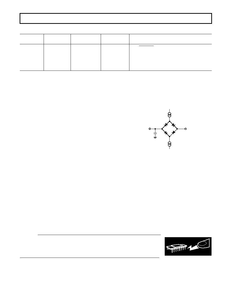
TO
OUTPUT
PIN
+2.1V
1.6mA
200A
50pF
Figure 1. Load Circuit for Access Time and Bus
Relinquish Time
WARNING!
ESD SENSITIVE DEVICE
CAUTION
ESD (electrostatic discharge) sensitive device. Electrostatic charges as high as 4000 V readily
accumulate on the human body and test equipment and can discharge without detection. Although
the AD7893 features proprietary ESD protection circuitry, permanent damage may occur on devices
subjected to high energy electrostatic discharges. Therefore, proper ESD precautions are
recommended to avoid performance degradation or loss of functionality.
相关PDF资料 |
PDF描述 |
|---|---|
| LTC1481IS8 | IC TXRX RS485 LOPWR W/SHTDN8SOIC |
| VE-2NV-MX-F1 | CONVERTER MOD DC/DC 5.8V 75W |
| MS3102E22-12SX | CONN RCPT 5POS BOX MNT W/SCKT |
| LT1785IN8 | IC TXRX RS485/RS422 60V 8-DIP |
| IDT7202LA35J8 | IC FIFO ASYNCH 1KX9 35NS 32PLCC |
相关代理商/技术参数 |
参数描述 |
|---|---|
| AD7893ANZ-10 | 功能描述:IC ADC 12BIT SRL T/H LP 8DIP RoHS:是 类别:集成电路 (IC) >> 数据采集 - 模数转换器 系列:- 标准包装:1 系列:- 位数:14 采样率(每秒):83k 数据接口:串行,并联 转换器数目:1 功率耗散(最大):95mW 电压电源:双 ± 工作温度:0°C ~ 70°C 安装类型:通孔 封装/外壳:28-DIP(0.600",15.24mm) 供应商设备封装:28-PDIP 包装:管件 输入数目和类型:1 个单端,双极 |
| AD7893ANZ-2 | 功能描述:IC ADC 12BIT SRL T/H LP 8-DIP RoHS:是 类别:集成电路 (IC) >> 数据采集 - 模数转换器 系列:- 标准包装:1 系列:microPOWER™ 位数:8 采样率(每秒):1M 数据接口:串行,SPI? 转换器数目:1 功率耗散(最大):- 电压电源:模拟和数字 工作温度:-40°C ~ 125°C 安装类型:表面贴装 封装/外壳:24-VFQFN 裸露焊盘 供应商设备封装:24-VQFN 裸露焊盘(4x4) 包装:Digi-Reel® 输入数目和类型:8 个单端,单极 产品目录页面:892 (CN2011-ZH PDF) 其它名称:296-25851-6 |
| AD7893ANZ-5 | 功能描述:IC ADC 12BIT SRL T/H LP 8DIP RoHS:是 类别:集成电路 (IC) >> 数据采集 - 模数转换器 系列:- 其它有关文件:TSA1204 View All Specifications 标准包装:1 系列:- 位数:12 采样率(每秒):20M 数据接口:并联 转换器数目:2 功率耗散(最大):155mW 电压电源:模拟和数字 工作温度:-40°C ~ 85°C 安装类型:表面贴装 封装/外壳:48-TQFP 供应商设备封装:48-TQFP(7x7) 包装:Digi-Reel® 输入数目和类型:4 个单端,单极;2 个差分,单极 产品目录页面:1156 (CN2011-ZH PDF) 其它名称:497-5435-6 |
| AD7893AR-10 | 功能描述:IC ADC 12BIT SRL T/H LP 8-SOIC RoHS:否 类别:集成电路 (IC) >> 数据采集 - 模数转换器 系列:- 标准包装:1,000 系列:- 位数:12 采样率(每秒):300k 数据接口:并联 转换器数目:1 功率耗散(最大):75mW 电压电源:单电源 工作温度:0°C ~ 70°C 安装类型:表面贴装 封装/外壳:24-SOIC(0.295",7.50mm 宽) 供应商设备封装:24-SOIC 包装:带卷 (TR) 输入数目和类型:1 个单端,单极;1 个单端,双极 |
| AD7893AR-10REEL | 功能描述:IC ADC 12BIT SRL T/H LP 8-SOIC RoHS:否 类别:集成电路 (IC) >> 数据采集 - 模数转换器 系列:- 标准包装:1,000 系列:- 位数:12 采样率(每秒):300k 数据接口:并联 转换器数目:1 功率耗散(最大):75mW 电压电源:单电源 工作温度:0°C ~ 70°C 安装类型:表面贴装 封装/外壳:24-SOIC(0.295",7.50mm 宽) 供应商设备封装:24-SOIC 包装:带卷 (TR) 输入数目和类型:1 个单端,单极;1 个单端,双极 |
发布紧急采购,3分钟左右您将得到回复。