- 您现在的位置:买卖IC网 > PDF目录10113 > AD7893BN-10 (Analog Devices Inc)IC ADC 12BIT SRL T/H LP 8-DIP PDF资料下载
参数资料
| 型号: | AD7893BN-10 |
| 厂商: | Analog Devices Inc |
| 文件页数: | 11/12页 |
| 文件大小: | 0K |
| 描述: | IC ADC 12BIT SRL T/H LP 8-DIP |
| 标准包装: | 1 |
| 位数: | 12 |
| 采样率(每秒): | 117k |
| 数据接口: | 串行 |
| 转换器数目: | 1 |
| 功率耗散(最大): | 45mW |
| 电压电源: | 单电源 |
| 工作温度: | -40°C ~ 85°C |
| 安装类型: | 通孔 |
| 封装/外壳: | 8-DIP(0.300",7.62mm) |
| 供应商设备封装: | 8-PDIP |
| 包装: | 管件 |
| 输入数目和类型: | 1 个单端,双极 |
AD7893
REV. E
–8–
This scheme limits the throughput rate to 12
s minimum; how-
ever, depending on the response time of the microprocessor to
the interrupt signal and the time taken by the processor to read
the data, this may be the fastest the system could have operated.
In any case, the CONVST signal does not have to have a 50:50
duty cycle. This can be tailored to optimize the throughput rate
of the part for a given system.
Alternatively, the CONVST signal can be used as a normal narrow
pulse width. The rising edge of CONVST can be used as an active
high or rising edge-triggered interrupt. A software delay of 6
s can
then be implemented before data is read from the part.
Serial Interface
The serial interface to the AD7893 consists of just two wires, a
serial clock input (SCLK) and the serial data output (SDATA).
This allows for an easy to use interface to most microcontrollers,
DSP processors and shift registers.
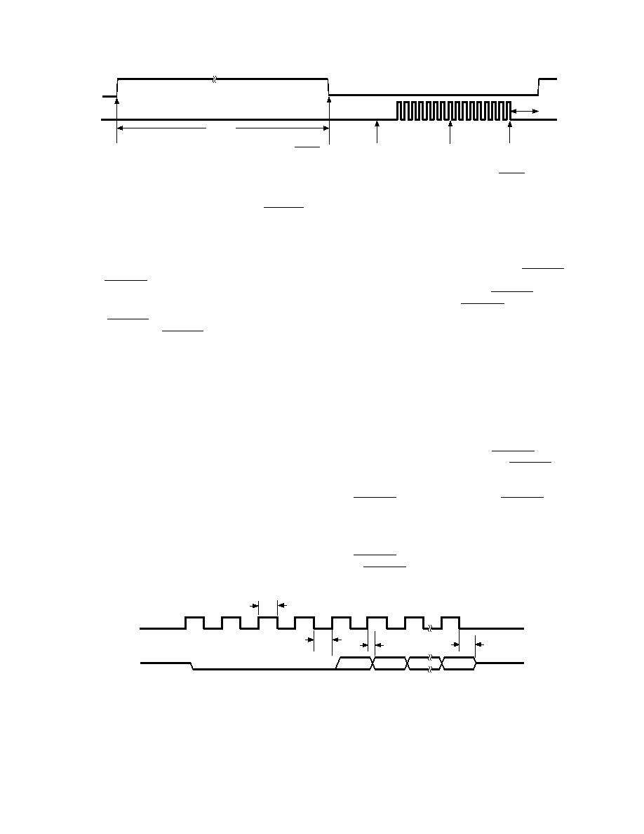
Figure 5 shows the timing diagram for the read operation to the
AD7893. The serial clock input (SCLK) provides the clock
source for the serial interface. Serial data is clocked out from the
SDATA line on the rising edge of this clock and is valid on the
falling edge of SCLK. Sixteen clock pulses must be provided to
the part to access to full conversion result. The AD7893 pro-
vides four leading zeros followed by the 12-bit conversion result
starting with the MSB (DB11). The last data bit to be clocked
out on the final rising clock edge is the LSB (DB0). On the six-
teenth falling edge of SCLK, the SDATA line is disabled (three-
stated). After this last bit has been clocked out, the SCLK input
should return low and remain low until the next serial data read
operation. If there are extra clock pulses after the sixteenth
clock, the AD7893 will start over again with outputting data
from its output register, and the data bus will no longer be
three-stated even when the clock stops. Provided that the serial
clock has stopped before the next falling edge of CONVST, the
AD7893 will continue to operate correctly with the output shift
register being reset on the falling edge of CONVST; however,
the SCLK line must be low when CONVST goes low in order
to reset the output shift register correctly.
The serial clock input does not have to be continuous during the
serial read operation. The sixteen bits of data (four leading zeros
and 12 bit conversion result) can be read from the AD7893 in a
number of bytes; however, the SCLR input must remain low be-
tween the two bytes.
Normally, the output register is updated at the end of conver-
sion. If a serial read from the output register is in progress when
conversion is complete; however, the updating of the output
register is deferred. In this case, the output register is updated
when the serial read is completed. If the serial read has not been
completed before the next falling edge of CONVST, the output
register will be updated on the falling edge of CONVST, and
the output shift register count is reset. In applications where the
data read has been started and not completed before the falling
edge of CONVST, the user must provide a CONVST pulse
width of greater than 1.5
s to ensure correct setup of the AD7893
before the next conversion is initiated. In applications where the
output update takes place either at the end of conversion or at
the end of a serial read that is completed 1.5
s before the rising
edge of CONVST, the normal pulse width of 50 ns minimum
applies to CONVST.
CONVST
SCLK
CONVERSION IS INITIATED
AND TRACK/HOLD GOES
INTO HOLD
CONVST INDICATES
TO P THAT
CONVERSION IS
COMPLETE
tCONVERT
SERIAL READ
OPERATION
P INT SERVICE
OR POLLING
ROUTINE
600ns MIN
READ OPERATION
SHOULD END 600ns
PRIOR TO NEXT
RISING EDGE OF
CONVST
Figure 4. CONVST Used as Status Signal
SDATA (O)
SCLK (I)
FOUR LEADING ZEROS
DB11
DB10
THREE-STATE
DB0
t5
t4
t3
t2
Figure 5. Data Read Operation
相关PDF资料 |
PDF描述 |
|---|---|
| MS27497T18F35S | CONN RCPT 66POS WALL MNT W/SCKT |
| VI-BN0-MW-F4 | CONVERTER MOD DC/DC 5V 100W |
| LTC2864CS-1#PBF | IC TRANSCEIVER RS485 14-SOIC |
| PX0941/10/P | CONN BOX MOUNT 10POS W/PINS |
| VI-BN0-MW-F3 | CONVERTER MOD DC/DC 5V 100W |
相关代理商/技术参数 |
参数描述 |
|---|---|
| AD7893BN-2 | 制造商:Rochester Electronics LLC 功能描述:12-BIT ADC, 8 PIN PACKAGE - Bulk 制造商:Analog Devices 功能描述: |
| AD7893BN-5 | 制造商:Rochester Electronics LLC 功能描述:12-BIT ADC,8-PIN I.C. - Bulk 制造商:Analog Devices 功能描述: |
| AD7893BNZ-10 | 功能描述:IC ADC 12BIT SRL T/H LP 8DIP RoHS:是 类别:集成电路 (IC) >> 数据采集 - 模数转换器 系列:- 标准包装:1 系列:- 位数:14 采样率(每秒):83k 数据接口:串行,并联 转换器数目:1 功率耗散(最大):95mW 电压电源:双 ± 工作温度:0°C ~ 70°C 安装类型:通孔 封装/外壳:28-DIP(0.600",15.24mm) 供应商设备封装:28-PDIP 包装:管件 输入数目和类型:1 个单端,双极 |
| AD7893BNZ-2 | 功能描述:IC ADC 12BIT SRL T/H LP 8DIP RoHS:是 类别:集成电路 (IC) >> 数据采集 - 模数转换器 系列:- 标准包装:1 系列:- 位数:14 采样率(每秒):83k 数据接口:串行,并联 转换器数目:1 功率耗散(最大):95mW 电压电源:双 ± 工作温度:0°C ~ 70°C 安装类型:通孔 封装/外壳:28-DIP(0.600",15.24mm) 供应商设备封装:28-PDIP 包装:管件 输入数目和类型:1 个单端,双极 |
| AD7893BNZ-5 | 制造商:Analog Devices 功能描述:ADC Single SAR 117ksps 12-bit Serial 8-Pin PDIP |
发布紧急采购,3分钟左右您将得到回复。