- 您现在的位置:买卖IC网 > PDF目录10113 > AD7893BN-10 (Analog Devices Inc)IC ADC 12BIT SRL T/H LP 8-DIP PDF资料下载
参数资料
| 型号: | AD7893BN-10 |
| 厂商: | Analog Devices Inc |
| 文件页数: | 9/12页 |
| 文件大小: | 0K |
| 描述: | IC ADC 12BIT SRL T/H LP 8-DIP |
| 标准包装: | 1 |
| 位数: | 12 |
| 采样率(每秒): | 117k |
| 数据接口: | 串行 |
| 转换器数目: | 1 |
| 功率耗散(最大): | 45mW |
| 电压电源: | 单电源 |
| 工作温度: | -40°C ~ 85°C |
| 安装类型: | 通孔 |
| 封装/外壳: | 8-DIP(0.300",7.62mm) |
| 供应商设备封装: | 8-PDIP |
| 包装: | 管件 |
| 输入数目和类型: | 1 个单端,双极 |
AD7893
REV. E
–6–
CONVERTER DETAILS
The AD7893 is a fast, 12-bit single supply A/D converter. It
provides the user with signal scaling (AD7893-10), track/hold,
A/D converter and serial interface logic functions on a single
chip. The A/D converter section of the AD7893 consists of a
conventional successive-approximation converter based on an
R-2R ladder structure. The signal scaling on the AD7893-10,
AD7893-5 and AD7893-3 allows the part to handle
±10 V, 0 V
to +5 V and
±2.5 V input signals, respectively, while operating
from a single +5 V supply. The AD7893-2 accepts an analog in-
put range of 0 V to +2.5 V. The part requires an external +2.5 V
reference. The reference input to the part is buffered on-chip.
A major advantage of the AD7893 is that it provides all of the
above functions in an 8-pin package, either 8-pin mini-DIP or
SOIC. This offers the user considerable space saving advantages
over alternative solutions. The AD7893 typically consumes only
25 mW, making it ideal for battery-powered applications.
Conversion is initiated on the AD7893 by pulsing the CONVST
input. On the rising edge of CONVST, the on-chip track/hold
goes from track-to-hold mode and the conversion sequence is
started. The conversion clock for the part is generated internally
using a laser-trimmed clock oscillator circuit. Conversion time
for the AD7893 is 6
s, and the track/hold acquisition time is
1.5
s. To obtain optimum performance from the part, the read
operation should not occur during the conversion or during
600 ns prior to the next conversion. This allows the part to op-
erate at throughput rates up to 117 kHz and to achieve data
sheet specifications. The part can operate at higher throughput
rates (up to 133 kHz) with slightly degraded performance (see
Timing and Control section).
CIRCUIT DESCRIPTION
Analog Input Section
The AD7893 is offered as four part types: the AD7893-10,
which handles a
±10 V input voltage range; the AD7893-3,
which handles a
±2.5 V input voltage range; the AD7893-5,
which handles a 0 V to +5 V input range; and the AD7893-2,
which handles a 0 V to +2.5 V input voltage range.
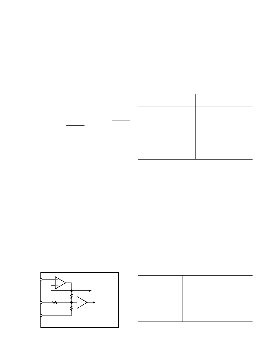
Figure 2 shows the analog input section for the AD7893-10,
AD7893-5 and AD7893-3. The analog input range of the
AD7893-10 is
±10 V into an input resistance of typically 33 k.
The analog input range of the AD7893-3 is
±2.5 V into an input
resistance of typically 12 k
. The input range on the AD7893-5 is
0 V to +5 V into an input resistance of typically 11 k
. This in-
put is benign with no dynamic charging currents, as the resistor
stage is followed by a high input impedance stage of the track/hold
AGND
AD7893-10/AD7893-5
VIN
REF IN
TRACK/
HOLD
TO ADC
REFERENCE
CIRCUITRY
TO INTERNAL
COMPARATOR
R3
R2
R1
Figure 2. AD7893-10/AD7893-3/AD7893-5 Analog Input
Structure
amplifier. For the AD7893-10, R1 = 30 k
; R2 = 7.5 k and
R3 = 10 k
. For the AD7893-3, R1 = R2 = 6.5 k, and R3
is open circuit. For the AD7893-5, R1 and R3 = 5 k
while
R2 is open-circuit.
For the AD7893-10 and AD7893-3, the designed code transi-
tions occur on successive integer LSB values (i.e., 1 LSB, 2 LSBs,
3 LSBs . . .). Output coding is twos complement binary with
1 LSB = FS/4096. The ideal input/output transfer function for
the AD7893-10 and AD7893-3 is shown in Table I.
Table I. Ideal Input/Output Code Table for the AD7893-10/
AD7893-3
Digital Output
Analog Input
1
Code Transition
+FSR/2 – 1 LSB
2
011 . . . 110 to 011 . . . 111
+FSR/2 – 2 LSBs
011 . . . 101 to 011 . . . 110
+FSR/2 – 3 LSBs
011 . . . 100 to 011 . . . 101
AGND + 1 LSB
000 . . . 000 to 000 . . . 001
AGND
111 . . . 111 to 000 . . . 000
AGND – 1 LSB
111 . . . 110 to 111 . . . 111
–FSR/2 + 3 LSBs
100 . . . 010 to 100 . . . 011
–FSR/2 + 2 LSBs
100 . . . 001 to 100 . . . 010
–FSR/2 + 1 LSB
100 . . . 000 to 100 . . . 001
NOTES
1FSR is full-scale range and is 20 V (AD7893-10) and = 5 V (AD7893-3) with
REF IN = +2.5 V.
21 LSB = FSR/4096 = 4.883 mV (AD7893-10) and 1.22 mV (AD7893-3) with
REF IN = +2.5 V.
For the AD7893-5, the designed code transitions occur again on
successive integer LSB values. Output coding is straight (natural)
binary with 1 LSB = FS/4096 = 5 V/4096 = 1.22 mV. The ideal
input/output transfer function for the AD7893-5 is shown in
Table II.
The analog input section for the AD7893-2 contains no biasing
resistors, and the VIN pin drives the input directly to the track/
hold amplifier. The analog input range is 0 V to +2.5 V into a
high impedance stage, with an input current of less than
500 nA. This input is benign, with no dynamic charging cur-
rents. Once again, the designed code transitions occur on suc-
cessive integer LSB values. Output coding is straight (natural)
binary with 1 LSB = FS/4096 = 2.5 V/4096 = 0.61 mV. Table
II also shows the ideal input/output transfer function for the
AD7893-2.
Table II. Ideal Input/Output Code Table for
AD7893-2/AD7893-5
Digital Output
Analog Input
1
Code Transition
+FSR – 1 LSB2
111 . . . 110 to 111 . . . 111
+FSR – 2 LSB
111 . . . 101 to 111 . . . 110
+FSR – 3 LSB
111 . . . 100 to 111 . . . 101
AGND + 3 LSB
000 . . . 010 to 000 . . . 011
AGND + 2 LSB
000 . . . 001 to 000 . . . 010
AGND + 1 LSB
000 . . . 000 to 000 . . . 001
NOTES
1FSR is Full-Scale Range and is 5 V for AD7893-5 and 2.5 V for AD7893-2
with REF IN = +2.5 V.
21 LSB = FSR/4096 and is 1.22 mV for AD7893-5 and 0.61 mV for AD7893-2
with REF IN = +2.5 V.
相关PDF资料 |
PDF描述 |
|---|---|
| MS27497T18F35S | CONN RCPT 66POS WALL MNT W/SCKT |
| VI-BN0-MW-F4 | CONVERTER MOD DC/DC 5V 100W |
| LTC2864CS-1#PBF | IC TRANSCEIVER RS485 14-SOIC |
| PX0941/10/P | CONN BOX MOUNT 10POS W/PINS |
| VI-BN0-MW-F3 | CONVERTER MOD DC/DC 5V 100W |
相关代理商/技术参数 |
参数描述 |
|---|---|
| AD7893BN-2 | 制造商:Rochester Electronics LLC 功能描述:12-BIT ADC, 8 PIN PACKAGE - Bulk 制造商:Analog Devices 功能描述: |
| AD7893BN-5 | 制造商:Rochester Electronics LLC 功能描述:12-BIT ADC,8-PIN I.C. - Bulk 制造商:Analog Devices 功能描述: |
| AD7893BNZ-10 | 功能描述:IC ADC 12BIT SRL T/H LP 8DIP RoHS:是 类别:集成电路 (IC) >> 数据采集 - 模数转换器 系列:- 标准包装:1 系列:- 位数:14 采样率(每秒):83k 数据接口:串行,并联 转换器数目:1 功率耗散(最大):95mW 电压电源:双 ± 工作温度:0°C ~ 70°C 安装类型:通孔 封装/外壳:28-DIP(0.600",15.24mm) 供应商设备封装:28-PDIP 包装:管件 输入数目和类型:1 个单端,双极 |
| AD7893BNZ-2 | 功能描述:IC ADC 12BIT SRL T/H LP 8DIP RoHS:是 类别:集成电路 (IC) >> 数据采集 - 模数转换器 系列:- 标准包装:1 系列:- 位数:14 采样率(每秒):83k 数据接口:串行,并联 转换器数目:1 功率耗散(最大):95mW 电压电源:双 ± 工作温度:0°C ~ 70°C 安装类型:通孔 封装/外壳:28-DIP(0.600",15.24mm) 供应商设备封装:28-PDIP 包装:管件 输入数目和类型:1 个单端,双极 |
| AD7893BNZ-5 | 制造商:Analog Devices 功能描述:ADC Single SAR 117ksps 12-bit Serial 8-Pin PDIP |
发布紧急采购,3分钟左右您将得到回复。