- 您现在的位置:买卖IC网 > PDF目录10363 > AD7904BRUZ-REEL7 (Analog Devices Inc)IC ADC 8BIT 4CH W/SEQ 16TSSOP PDF资料下载
参数资料
| 型号: | AD7904BRUZ-REEL7 |
| 厂商: | Analog Devices Inc |
| 文件页数: | 13/32页 |
| 文件大小: | 0K |
| 描述: | IC ADC 8BIT 4CH W/SEQ 16TSSOP |
| 标准包装: | 1,000 |
| 位数: | 8 |
| 采样率(每秒): | 1M |
| 数据接口: | DSP,MICROWIRE?,QSPI?,串行,SPI? |
| 转换器数目: | 1 |
| 功率耗散(最大): | 13.5mW |
| 电压电源: | 单电源 |
| 工作温度: | -40°C ~ 85°C |
| 安装类型: | 表面贴装 |
| 封装/外壳: | 16-TSSOP(0.173",4.40mm 宽) |
| 供应商设备封装: | 16-TSSOP |
| 包装: | 带卷 (TR) |
| 输入数目和类型: | 4 个单端,单极 |
| 配用: | EVAL-AD79X4CBZ-ND - BOARD EVALUATION FOR AD79X4CBZ |
第1页第2页第3页第4页第5页第6页第7页第8页第9页第10页第11页第12页当前第13页第14页第15页第16页第17页第18页第19页第20页第21页第22页第23页第24页第25页第26页第27页第28页第29页第30页第31页第32页
AD7904/AD7914/AD7924
Data Sheet
Rev. C | Page 20 of 32
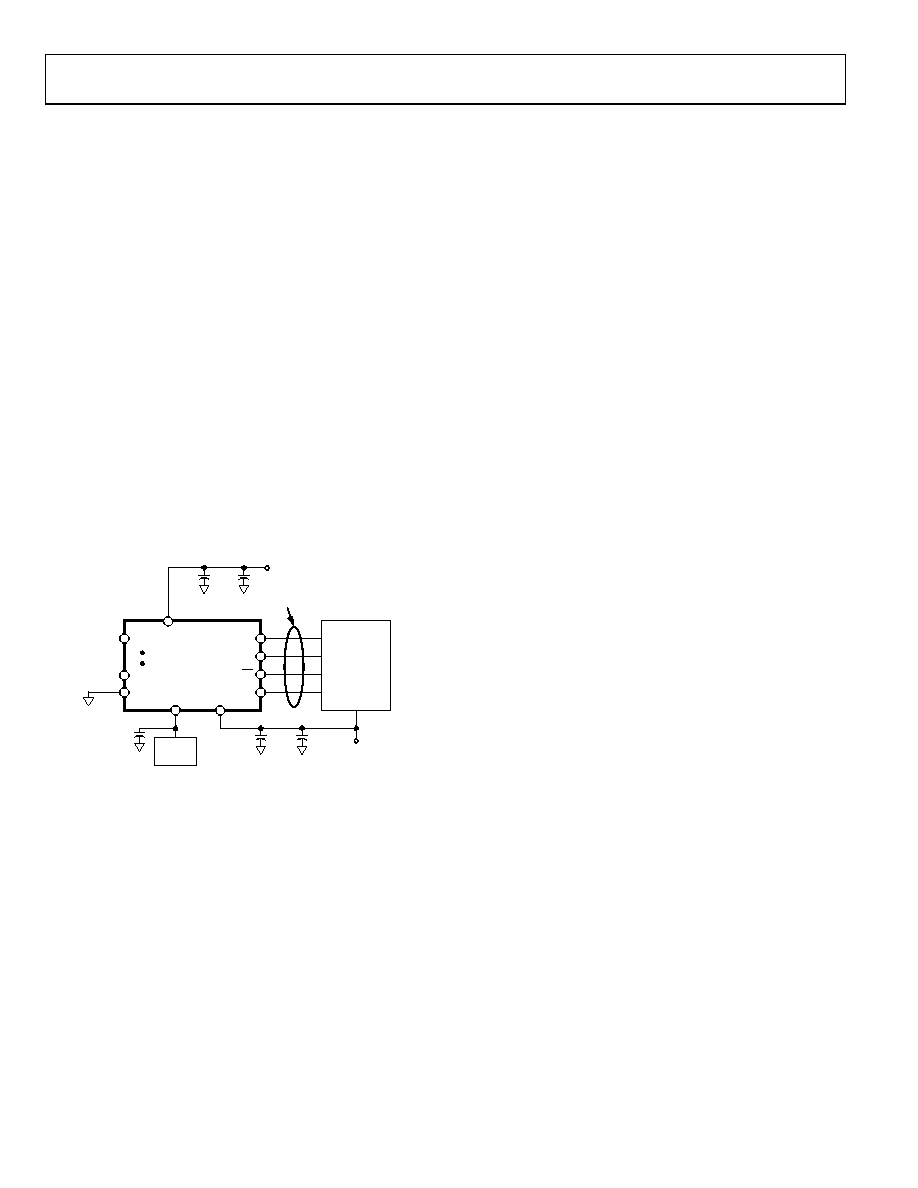
TYPICAL CONNECTION DIAGRAM
Figure 19 shows a typical connection diagram for the AD7904/
AD7914/AD7924. In this setup, the AGND pin is connected to
the analog ground plane of the system. In Figure 19, the REFIN
pin is connected to a decoupled 2.5 V supply from a reference
source, the AD780, to provide an analog input range of 0 V to
2.5 V (if the RANGE bit is set to 1) or 0 V to 5 V (if the RANGE
bit is set to 0).
Although the AD7904/AD7914/AD7924 are connected to a VDD
of 5 V, the serial interface is connected to a 3 V microprocessor.
The VDRIVE pin of the AD7904/AD7914/AD7924 is connected to
the same 3 V supply as the microprocessor to allow a 3 V logic
interface (see the Digital Inputs section). The conversion result
is output in a 16-bit word. This 16-bit data stream consists of
two leading zeros, two address bits indicating which channel the
conversion result corresponds to, followed by the 12 bits of
conversion data for the AD7924 (10 bits of data for the AD7914
and 8 bits of data for the AD7904, each followed by two and
four trailing zeros, respectively). For applications where power
consumption is of concern, the power-down modes should be
used between conversions or bursts of several conversions to
improve power performance (see the Modes of Operation
section).
NOTES
1. ALL UNUSED INPUT CHANNELS SHOULD BE CONNECTED TO AGND.
VIN0
VIN3
AGND
SCLK
DOUT
CS
DIN
AD7904/
AD7914/
AD7924
0V TO REFIN
REFIN
VDRIVE
AVDD
0.1F
10F
5V
SUPPLY
SERIAL
INTERFACE
0.1F
10F
MICRO-
CONTROLLER/
MICRO-
PROCESSOR
2.5V
AD780
3V SUPPLY
03087-
019
Figure 19. Typical Connection Diagram
Analog Input Selection
Any one of four analog input channels can be selected for
conversion by programming the multiplexer with the address
bits ADD1 and ADD0 in the control register. The channel
configurations are shown in Table 7.
The AD7904/AD7914/AD7924 can also be configured to auto-
matically cycle through a number of selected channels. The
sequencer feature is accessed via the SEQ1 and SEQ0 bits in the
control register (see Table 10). The AD7904/AD7914/AD7924
can be programmed to continuously convert on a number of
consecutive channels in ascending order from Channel 0 to a
selected final channel as determined by the channel address
bits, ADD1 and ADD0. This is possible if the SEQ1 and SEQ0
bits are set to 11. The next serial transfer will then act on the
sequence programmed by executing a conversion on Channel 0.
The next serial transfer will result in a conversion on Channel 1,
and so on, until the channel selected via the address bits, ADD1
and ADD0, is reached.
It is not necessary to write to the control register again after a
sequence operation has been initiated. To ensure that the control
register is not accidently overwritten or the sequence operation
interrupted, the WRITE bit must be set to 0 or the DIN line
must be tied low. If the control register is written to at any time
during the sequence, the SEQ1 and SEQ0 bits must be set to 10
to avoid interrupting the automatic conversion sequence. This
pattern continues until the AD7904/AD7914/AD7924 are
written to and the SEQ1 and SEQ0 bits are configured with a bit
combination other than 10, resulting in the termination of the
sequence. If the sequence is uninterrupted (WRITE bit = 0, or
WRITE bit = 1 and SEQ1 and SEQ0 bits are set to 10), then upon
completion of the sequence, the AD7904/AD7914/AD7924
sequencer returns to Channel 0 and restarts the sequence.
Regardless of the channel selection method used, the 16-bit
word output from the AD7924 during each conversion always
contains two leading zeros, two channel address bits that the
conversion result corresponds to, followed by the 12-bit con-
version result; the AD7914 outputs two leading zeros, two
channel address bits that the conversion result corresponds to,
followed by the 10-bit conversion result and two trailing zeros;
the AD7904 outputs two leading zeros, two channel address bits
that the conversion result corresponds to, followed by the 8-bit
conversion result and four trailing zeros (see the Serial Interface
section).
相关PDF资料 |
PDF描述 |
|---|---|
| MS27468T23B21A | CONN HSG RCPT 21POS JAMNUT PINS |
| ISL54005IRTZ | IC AMP AUDIO PWR 1.23W AB 20TQFN |
| VE-J5J-MX | CONVERTER MOD DC/DC 36V 75W |
| VE-J54-MX | CONVERTER MOD DC/DC 48V 75W |
| VI-B4W-IV-F2 | CONVERTER MOD DC/DC 5.5V 150W |
相关代理商/技术参数 |
参数描述 |
|---|---|
| AD7904WYRUZ-REEL7 | 功能描述:IC ADC 8BIT 4CH W/SEQ 16TSSOP RoHS:是 类别:集成电路 (IC) >> 数据采集 - 模数转换器 系列:- 标准包装:2,500 系列:- 位数:16 采样率(每秒):15 数据接口:MICROWIRE?,串行,SPI? 转换器数目:1 功率耗散(最大):480µW 电压电源:单电源 工作温度:-40°C ~ 85°C 安装类型:表面贴装 封装/外壳:38-WFQFN 裸露焊盘 供应商设备封装:38-QFN(5x7) 包装:带卷 (TR) 输入数目和类型:16 个单端,双极;8 个差分,双极 配用:DC1011A-C-ND - BOARD DELTA SIGMA ADC LTC2494 |
| AD7908 | 制造商:AD 制造商全称:Analog Devices 功能描述:8-Channel, 1 MSPS, 8-/10-/12-Bit ADCs with Sequencer in 20-Lead TSSOP |
| AD7908BRU | 制造商:Analog Devices 功能描述:ADC Single SAR 1Msps 8-bit Serial 20-Pin TSSOP 制造商:Rochester Electronics LLC 功能描述:8-BIT 8, CH 1 MSPS ADC - Bulk 制造商:Analog Devices 功能描述:IC 8BIT ADC SMD 7908 TSSOP20 |
| AD7908BRU-REEL | 制造商:Analog Devices 功能描述:ADC Single SAR 1Msps 8-bit Serial 20-Pin TSSOP T/R 制造商:Analog Devices 功能描述:ADC SGL SAR 1MSPS 8BIT SERL 20TSSOP - Tape and Reel |
| AD7908BRU-REEL7 | 制造商:Analog Devices 功能描述:ADC Single SAR 1Msps 8-bit Serial 20-Pin TSSOP T/R 制造商:Analog Devices 功能描述:ADC SGL SAR 1MSPS 8BIT SERL 20TSSOP - Tape and Reel |
发布紧急采购,3分钟左右您将得到回复。