参数资料
| 型号: | AD790SQ |
| 厂商: | Analog Devices Inc |
| 文件页数: | 7/12页 |
| 文件大小: | 0K |
| 描述: | IC COMPARATOR PREC W/LATCH 8CDIP |
| 设计资源: | Automated Calibration Technique That Reduces AD5360 Offset Voltage to Less Than 1 mV (CN0123) |
| 标准包装: | 1 |
| 类型: | 带锁销 |
| 元件数: | 1 |
| 输出类型: | CMOS,TTL |
| 电压 - 电源,单路/双路(±): | 4.5 V ~ 7 V,±2.25 V ~ 16.5 V |
| 电压 - 输入偏移(最小值): | 1.5mV @ 5V |
| 电流 - 输入偏压(最小值): | 5µA @ 5V |
| 电流 - 静态(最大值): | 10mA |
| CMRR, PSRR(标准): | 95dB CMRR,90dB PSRR |
| 传输延迟(最大): | 50ns |
| 磁滞: | 500µV |
| 工作温度: | -55°C ~ 125°C |
| 封装/外壳: | 8-CDIP(0.300",7.62mm) |
| 安装类型: | 通孔 |
| 包装: | 管件 |
AD790
REV. D
–4–
ABSOLUTE MAXIMUM RATINGS
1, 2
Supply Voltage . . . . . . . . . . . . . . . . . . . . . . . . . . . . . . . .
±18 V
Internal Power Dissipation
2
. . . . . . . . . . . . . . . . . . . 500 mW
Differential Input Voltage . . . . . . . . . . . . . . . . . . . . .
±16.5 V
Output Short-Circuit Duration . . . . . . . . . . . . . . . . Indefinite
Storage Temperature Range
(N, R) . . . . . . . . . . . . . . . . . . . . . . . . . . . –65
°C to +125°C
(Q) . . . . . . . . . . . . . . . . . . . . . . . . . . . . . . –65
°C to +150°C
Lead Temperature Range (Soldering 60 sec) . . . . . . . . 300
°C
Logic Supply Voltage . . . . . . . . . . . . . . . . . . . . . . . . . . . . . 7 V
NOTES
1Stresses above those listed under “Absolute Maximum Ratings” may cause perma-
nent damage to the device. This is a stress rating only and functional operation of
the device at these or any other conditions above those indicated in the operational
sections of this specification is not implied. Exposure to absolute maximum rating
conditions for extended periods may affect device reliability.
2Thermal characteristics: plastic N-8 package:
θ
JA = 90
°C/watt; ceramic Q-8
package:
θ
JA = 110
°C/watt, θ
JC = 30
°C/watt. SOIC (R-8) package: θ
JA = 160
°C
watt;
θ
JC = 42
°C/watt.
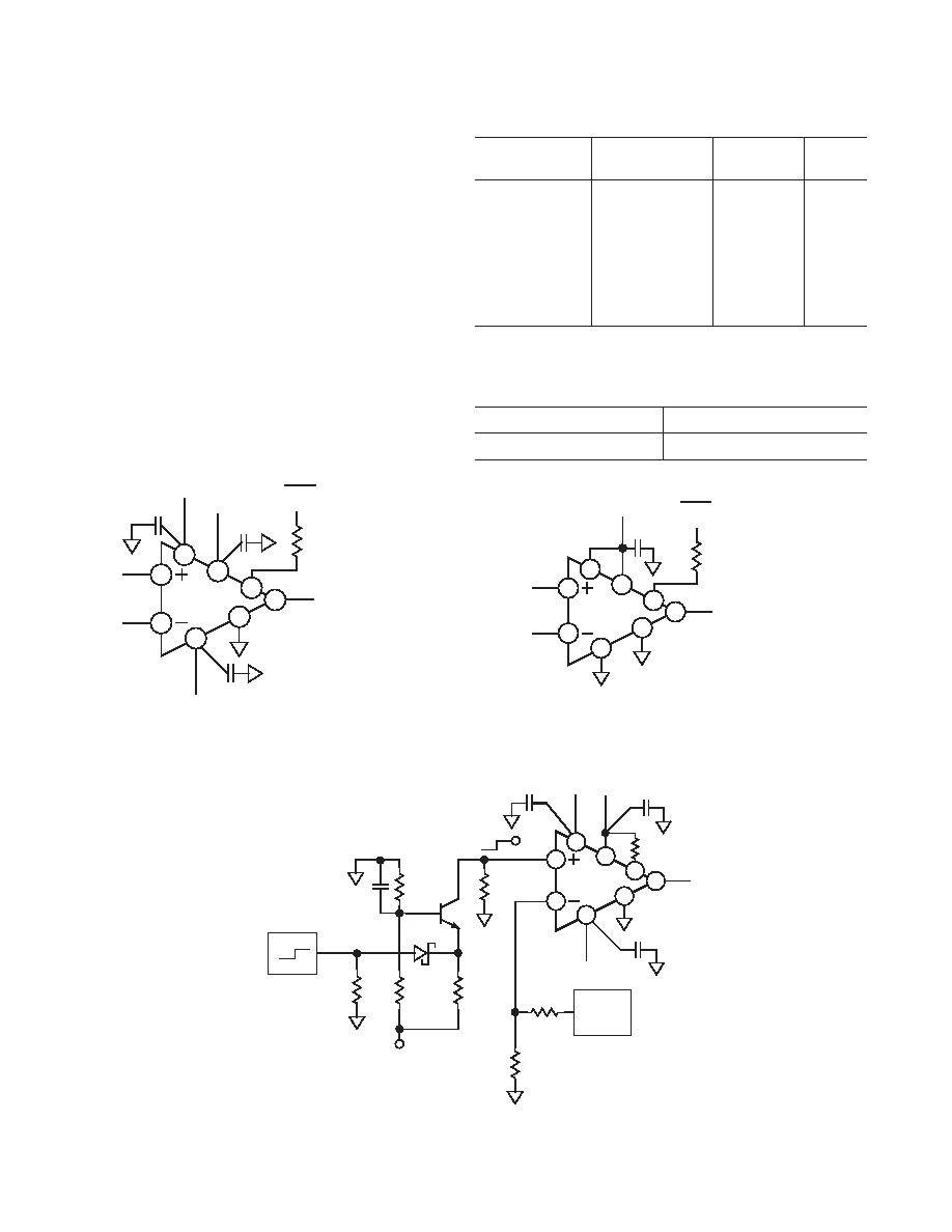
AD790
0.1F
15V
+
+IN
–IN
5V
+
510
OUTPUT
15V
–
LATCH
(OPTIONAL)
8
1
5
7
6
4
3
2
Figure 1. Basic Dual Supply
Configuration (N, Q Package Pinout)
AD790
1
2
3
4
5
6
7
8
+5V
+15V
–15V
TEK
7904
SCOPE
–5V
VOLTAGE
SOURCE
10
–5mV
0.1F
–100mV
–1.3V
–1.7V
–5V
HP8112
PULSE
GENERATOR
1k
HP2835
MPS
571
0.1F
10k
650
400
50
25
130
Figure 3. Response Time Test Circuit (N, Q Package Pinout)
ORDERING GUIDE
Temperature
Package
Model
Range
Description Option
AD790JN
0
°C to 70°C
Plastic DIP
N-8
AD790JR
0
°C to 70°C
SOIC
SO-8
AD790JR-REEL
0
°C to 70°C
Reel
AD790JR-REEL7 0
°C to 70°C
SOIC
R-8
AD790KN*
0
°C to 70°C
Plastic DIP
N-8
AD790AQ
–40
°C to +85°C
Cerdip
Q-8
AD790BQ*
–40
°C to +85°C
Cerdip
Q-8
AD790SQ
–55
°C to +125°C Cerdip
Q-8
*Not for new designs; obsolete April 2002.
For military processed devices, please refer to the standard Mi-
crocircuit Drawing (SMD) available at
www.dscc.dla.mil/programs/milspec/default.asp
SMD Part Number
ADI Equivalent
5962-9150501MPA*
AD790 SQ/883
*Not for new designs; obsolete April 2002.
AD790
1
2
3
4
5
6
7
8
0.1F
+IN
–IN
5V
+
OUTPUT
LATCH
(OPTIONAL)
510
Figure 2. Basic Single Supply
Configuration (N, Q Package Pinout)
相关PDF资料 |
PDF描述 |
|---|---|
| AD8013ANZ | IC OPAMP SINGLE 14DIP |
| AD8023ARZ | IC AMP VIDEO TRIPLE HC 14-SOIC |
| AD8073JNZ | IC VIDEO AMP TRIPLE 14-DIP |
| AD8074ARU | IC TRPL VID BUFF 500MHZ 16-TSSOP |
| AD810AN | IC CURR-FDBK AMP VIDEO LP 8-DIP |
相关代理商/技术参数 |
参数描述 |
|---|---|
| AD790SQ/883B | 制造商:AD 制造商全称:Analog Devices 功能描述:Fast, Precision Comparator |
| AD7910 | 制造商:AD 制造商全称:Analog Devices 功能描述:250 kSPS, 10-/12-Bit ADCs in 6-Lead SC70 |
| AD7910AKS-500RL7 | 制造商:Rochester Electronics LLC 功能描述: 制造商:Analog Devices 功能描述: |
| AD7910AKS-REEL | 制造商:Analog Devices 功能描述: |
| AD7910AKS-REEL7 | 制造商:Rochester Electronics LLC 功能描述: 制造商:Analog Devices 功能描述: |
发布紧急采购,3分钟左右您将得到回复。