- 您现在的位置:买卖IC网 > PDF目录10322 > AD7914WYRUZ-REEL7 (Analog Devices Inc)IC ADC 10BIT 4CH 1MSPS 16-TSSOP PDF资料下载
参数资料
| 型号: | AD7914WYRUZ-REEL7 |
| 厂商: | Analog Devices Inc |
| 文件页数: | 15/32页 |
| 文件大小: | 0K |
| 描述: | IC ADC 10BIT 4CH 1MSPS 16-TSSOP |
| 标准包装: | 1 |
| 位数: | 10 |
| 采样率(每秒): | 1M |
| 数据接口: | DSP,MICROWIRE?,QSPI?,串行,SPI? |
| 转换器数目: | 1 |
| 功率耗散(最大): | 13.5mW |
| 电压电源: | 单电源 |
| 安装类型: | 表面贴装 |
| 封装/外壳: | 16-TSSOP(0.173",4.40mm 宽) |
| 供应商设备封装: | 16-TSSOP |
| 包装: | 标准包装 |
| 输入数目和类型: | 4 个单端,单极 |
| 其它名称: | AD7914WYRUZ-REEL7DKR |
第1页第2页第3页第4页第5页第6页第7页第8页第9页第10页第11页第12页第13页第14页当前第15页第16页第17页第18页第19页第20页第21页第22页第23页第24页第25页第26页第27页第28页第29页第30页第31页第32页
AD7904/AD7914/AD7924
Data Sheet
Rev. C | Page 22 of 32
MODES OF OPERATION
The AD7904/AD7914/AD7924 have three modes of operation.
These modes are designed to provide flexible power management
options. These options can be chosen to optimize the power
dissipation/throughput rate ratio for differing application require-
ments. The mode of operation of the AD7904/AD7914/AD7924
is controlled by the power management bits, PM1 and PM0, in
the control register (see Table 9). When power supplies are first
applied to the AD7904/AD7914/AD7924, care should be taken to
ensure that the part is placed in the required mode of operation
(see the Powering Up the AD7904/AD7914/AD7924 section).
NORMAL MODE (PM1 = PM0 = 1)
Normal mode is intended for the fastest throughput rate perfor-
mance. Because the AD7904/AD7914/AD7924 remain fully
powered up at all times, the user does not need to worry about
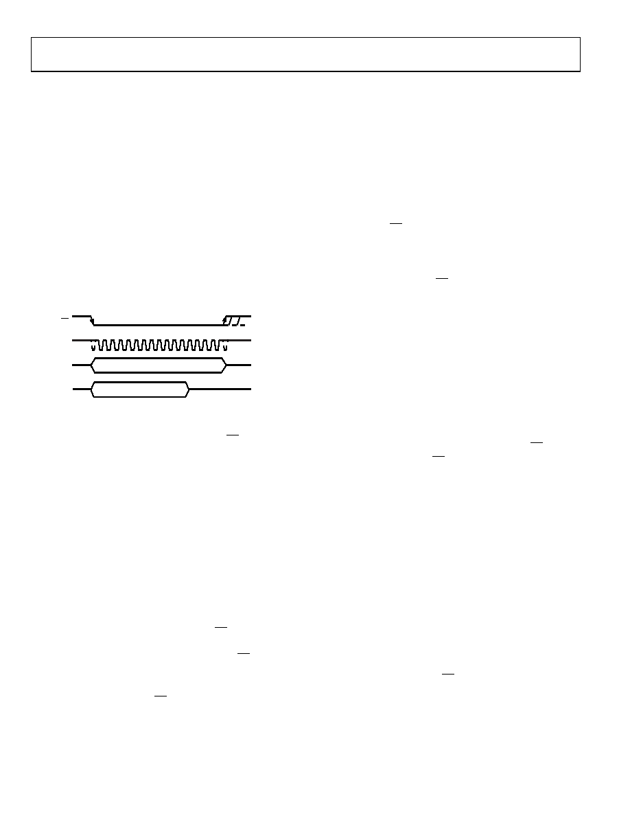
power-up times. Figure 20 shows the general diagram of the
operation of the AD7904/AD7914/AD7924 in this mode.
NOTES
1. CONTROL REGISTER DATA IS LOADED ON FIRST 12 SCLK CYCLES.
1
12
CS
SCLK
DOUT
DIN
16
DATA IN TO CONTROL REGISTER
2 LEADING ZEROS + 2 CHANNEL IDENTIFIER BITS
+ CONVERSION RESULT
03087-
020
Figure 20. Normal Mode Operation
The conversion is initiated on the falling edge of CS; the track-
and-hold enters hold mode as described in the Serial Interface
section. The data presented to the AD7904/AD7914/AD7924
on the DIN line during the first 12 clock cycles of the data
transfer is loaded into the control register (provided that the
WRITE bit is set to 1). In normal mode, the part remains fully
powered up at the end of the conversion as long as the PM1 and
PM0 bits are set to 1 in the write transfer during that same
conversion. To ensure continued operation in normal mode,
PM1 and PM0 must both be set to 1 on every data transfer,
assuming that a write operation is taking place. If the WRITE
bit is set to 0, the power management bits are left unchanged,
and the part remains in normal mode.
Sixteen serial clock cycles are required to complete the conversion
and to access the conversion result. The track-and-hold returns
to track mode on the 14th SCLK falling edge. CS may then idle
high until the next conversion or it may idle low until some
time prior to the next conversion (effectively idling CS low).
When a data transfer is complete (DOUT has returned to three-
state), another conversion can be initiated after the quiet time,
tQUIET, has elapsed by bringing CS low again.
FULL SHUTDOWN MODE (PM1 = 1, PM0 = 0)
In full shutdown mode, all internal circuitry on the AD7904/
AD7914/AD7924 is powered down. The part retains information
in the control register during full shutdown. The AD7904/AD7914/
AD7924 remain in full shutdown until the power management
bits in the control register, PM1 and PM0, are changed.
If a write to the control register occurs while the part is in full
shutdown, and the power management bits are changed to
PM0 = PM1 = 1 (that is, normal mode), the part will begin to
power up on the CS rising edge. The track-and-hold, which was
in hold mode while the part was in full shutdown, returns to
track mode on the 14th SCLK falling edge.
To ensure that the part is fully powered up, tPOWER-UP (t12) should
have elapsed before the next CS falling edge. Figure 21 shows
the general diagram for this sequence.
AUTO SHUTDOWN MODE (PM1 = 0, PM0 = 1)
In auto shutdown mode, the AD7904/AD7914/AD7924 auto-
matically enter shutdown at the end of each conversion when
the control register is updated. When the part is in auto shutdown,
the track-and-hold is in hold mode. Figure 22 shows the general
diagram of the operation of the AD7904/AD7914/AD7924 in
this mode.
In auto shutdown mode, all internal circuitry on the AD7904/
AD7914/AD7924 is powered down. The part retains information
in the control register during auto shutdown. The AD7904/
AD7914/AD7924 remain in shutdown until the next CS falling
edge that it receives. On this CS falling edge, the track-and-hold,
which was in hold mode while the part was in shutdown, returns
to track mode. Wake-up time from auto shutdown is 1 s max-
imum, and the user should ensure that 1 s has elapsed before
attempting a valid conversion.
When running the AD7904/AD7914/AD7924 with a 20 MHz
clock, one 16 SCLK dummy cycle should be sufficient to ensure
that the part is fully powered up. During this dummy cycle, the
contents of the control register should remain unchanged;
therefore, the WRITE bit should be set to 0 on the DIN line.
This dummy cycle effectively halves the throughput rate of the
part, with every other conversion result being valid. In auto
shutdown mode, the power consumption of the part is greatly
reduced because the part enters shutdown at the end of each
conversion. When the control register is programmed to move
into auto shutdown mode, it does so at the end of the con-
version. The user can move the ADC in and out of the low
power state by controlling the CS signal.
相关PDF资料 |
PDF描述 |
|---|---|
| LTC1199CMS8 | IC ADC 10BIT 450KHZ W/SD 8-MSOP |
| AD7933BRUZ-REEL7 | IC ADC 10BIT 4CH 1.5MSPS 28TSSOP |
| VI-27P-MX-S | CONVERTER MOD DC/DC 13.8V 75W |
| LTC2309CUF#TRPBF | IC ADC 12BIT SAR 24-QFN |
| D38999/20FC98SALC | CONN HSG RCPT 10POS WALL MT SCKT |
相关代理商/技术参数 |
参数描述 |
|---|---|
| AD7915BCPZ-RL7 | 功能描述:IC ADC 16BIT 1MSPS DIFF 10LFCSP 制造商:analog devices inc. 系列:PulSAR? 包装:剪切带(CT) 零件状态:在售 位数:16 采样率(每秒):1M 输入数:1 输入类型:差分 数据接口:SPI,DSP 配置:S/H-ADC 无线电 - S/H:ADC:1:1 A/D 转换器数:1 架构:SAR 参考类型:外部 电压 - 电源,模拟:2.375 V ~ 2.625 V 电压 - 电源,数字:2.375 V ~ 2.625 V 特性:- 工作温度:-40°C ~ 125°C 封装/外壳:10-WFDFN 裸露焊盘,CSP 供应商器件封装:10-LFCSP-WD(3x3) 标准包装:1 |
| AD7915BRMZ | 功能描述:16 Bit Analog to Digital Converter 1 Input 1 SAR 10-MSOP 制造商:analog devices inc. 系列:PulSAR? 包装:管件 零件状态:有效 位数:16 采样率(每秒):1M 输入数:1 输入类型:差分 数据接口:SPI,DSP 配置:S/H-ADC 无线电 - S/H:ADC:1:1 A/D 转换器数:1 架构:SAR 参考类型:外部 电压 - 电源,模拟:2.375 V ~ 2.625 V 电压 - 电源,数字:2.375 V ~ 2.625 V 特性:- 工作温度:-40°C ~ 125°C 封装/外壳:10-TFSOP,10-MSOP(0.118",3.00mm 宽) 供应商器件封装:10-MSOP 标准包装:1 |
| AD7915BRMZ-RL7 | 功能描述:16 Bit Analog to Digital Converter 1 Input 1 SAR 10-MSOP 制造商:analog devices inc. 系列:PulSAR? 包装:带卷(TR) 零件状态:有效 位数:16 采样率(每秒):1M 输入数:1 输入类型:差分 数据接口:SPI,DSP 配置:S/H-ADC 无线电 - S/H:ADC:1:1 A/D 转换器数:1 架构:SAR 参考类型:外部 电压 - 电源,模拟:2.375 V ~ 2.625 V 电压 - 电源,数字:2.375 V ~ 2.625 V 特性:- 工作温度:-40°C ~ 125°C 封装/外壳:10-TFSOP,10-MSOP(0.118",3.00mm 宽) 供应商器件封装:10-MSOP 标准包装:1,000 |
| AD7916BCPZ-RL7 | 功能描述:16 Bit Analog to Digital Converter 1 Input 1 SAR 10-LFCSP-WD (3x3) 制造商:analog devices inc. 系列:PulSAR? 包装:带卷(TR) 零件状态:有效 位数:16 采样率(每秒):500k 输入数:1 输入类型:差分 数据接口:SPI,DSP 配置:S/H-ADC 无线电 - S/H:ADC:1:1 A/D 转换器数:1 架构:SAR 参考类型:外部 电压 - 电源,模拟:2.375 V ~ 2.625 V 电压 - 电源,数字:2.375 V ~ 2.625 V 特性:- 工作温度:-40°C ~ 125°C 封装/外壳:10-WFDFN 裸露焊盘,CSP 供应商器件封装:10-LFCSP-WD(3x3) 标准包装:1,500 |
| AD7916BRMZ | 功能描述:16 Bit Analog to Digital Converter 1 Input 1 SAR 10-MSOP 制造商:analog devices inc. 系列:- 包装:管件 零件状态:有效 位数:16 采样率(每秒):500k 输入数:1 输入类型:差分 数据接口:SPI,DSP 配置:S/H-ADC 无线电 - S/H:ADC:1:1 A/D 转换器数:1 架构:SAR 参考类型:外部 电压 - 电源,模拟:2.375 V ~ 2.625 V 电压 - 电源,数字:2.375 V ~ 2.625 V 特性:- 工作温度:-40°C ~ 125°C 封装/外壳:10-TFSOP,10-MSOP(0.118",3.00mm 宽) 供应商器件封装:10-MSOP 标准包装:50 |
发布紧急采购,3分钟左右您将得到回复。