- 您现在的位置:买卖IC网 > PDF目录10322 > AD7914WYRUZ-REEL7 (Analog Devices Inc)IC ADC 10BIT 4CH 1MSPS 16-TSSOP PDF资料下载
参数资料
| 型号: | AD7914WYRUZ-REEL7 |
| 厂商: | Analog Devices Inc |
| 文件页数: | 18/32页 |
| 文件大小: | 0K |
| 描述: | IC ADC 10BIT 4CH 1MSPS 16-TSSOP |
| 标准包装: | 1 |
| 位数: | 10 |
| 采样率(每秒): | 1M |
| 数据接口: | DSP,MICROWIRE?,QSPI?,串行,SPI? |
| 转换器数目: | 1 |
| 功率耗散(最大): | 13.5mW |
| 电压电源: | 单电源 |
| 安装类型: | 表面贴装 |
| 封装/外壳: | 16-TSSOP(0.173",4.40mm 宽) |
| 供应商设备封装: | 16-TSSOP |
| 包装: | 标准包装 |
| 输入数目和类型: | 4 个单端,单极 |
| 其它名称: | AD7914WYRUZ-REEL7DKR |
第1页第2页第3页第4页第5页第6页第7页第8页第9页第10页第11页第12页第13页第14页第15页第16页第17页当前第18页第19页第20页第21页第22页第23页第24页第25页第26页第27页第28页第29页第30页第31页第32页
Data Sheet
AD7904/AD7914/AD7924
Rev. C | Page 25 of 32
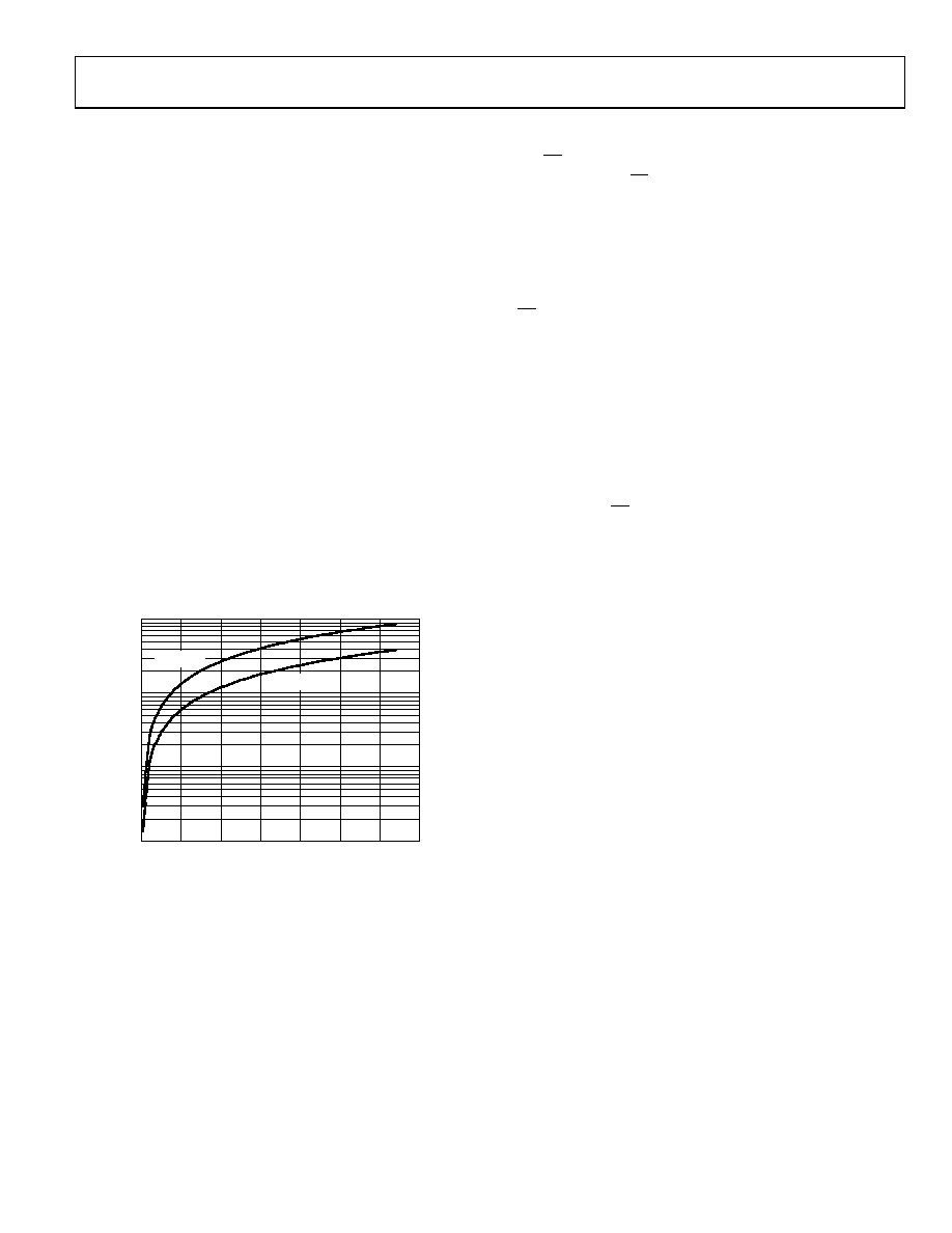
POWER vs. THROUGHPUT RATE
By operating the AD7904/AD7914/AD7924 in auto shutdown
mode, the average power consumption of the ADC decreases at
lower throughput rates. Figure 26 shows how, as the throughput
rate is reduced, the part remains in its shutdown state longer, and
the average power consumption over time drops accordingly.
For example, if the AD7924 is operated in continuous sampling
mode with a throughput rate of 100 kSPS and an SCLK of 20 MHz
(AVDD = 5 V), and the device is placed into auto shutdown mode
(PM1 = 0 and PM0 = 1), the power consumption is calculated
as described in this section.
The maximum power dissipation during normal operation is
13.5 mW (AVDD = 5 V). If the power-up time from auto shutdown
is one dummy cycle, that is, 1 s, and the remaining conversion
time is another cycle, that is, 1 s, then the AD7924 can be said
to dissipate 13.5 mW for 2 s during each conversion cycle. For
the remainder of the conversion cycle, 8 s, the part remains in
shutdown. The AD7924 can be said to dissipate 2.5 W for the
remaining 8 μs of the conversion cycle. If the throughput rate is
100 kSPS, the cycle time is 10 s and the average power dissipated
during each cycle is ((2/10) × 13.5 mW) + ((8/10) × 2.5 W) =
2.702 mW.
Figure 26 shows the maximum power vs. throughput rate when
using the auto shutdown mode with 5 V and 3 V supplies.
10
0.01
0.1
1
0
350
300
250
200
150
100
50
PO
W
ER
(m
W
)
THROUGHPUT (kSPS)
AVDD = 5V
AVDD = 3V
03087-
026
Figure 26. AD7924 Power vs. Throughput Rate
SERIAL INTERFACE
Figure 27, Figure 28, and Figure 29 show the detailed timing
diagrams for serial interfacing to the AD7904, AD7914, and
AD7924, respectively. The serial clock provides the conversion
clock and controls the transfer of information to and from the
AD7904/AD7914/AD7924 during each conversion.
The CS signal initiates the data transfer and conversion process.
The falling edge of CS puts the track-and-hold into hold mode
and takes the bus out of three-state; the analog input is sampled
at this point. The conversion is also initiated at this point and
requires 16 SCLK cycles to complete. The track-and-hold returns
to track mode on the 14th SCLK falling edge, as shown by Point B
in Figure 27, Figure 28, and Figure 29. On the 16th SCLK falling
edge, the DOUT line returns to three-state. If the rising edge of
CS occurs before 16 SCLKs have elapsed, the conversion is
terminated, the DOUT line returns to three-state, and the
control register is not updated; otherwise, DOUT returns to
three-state on the 16th SCLK falling edge, as shown in Figure 27,
Figure 28, and Figure 29.
Sixteen serial clock cycles are required to perform the conversion
process and to access data from the AD7904/AD7914/AD7924.
For the AD7904/AD7914/AD7924, the 8/10/12 bits of data are
preceded by two leading zeros and the two channel address bits,
ADD1 and ADD0, which identify the channel that the result
corresponds to. CS going low clocks out the first leading zero to
be read in by the microcontroller or DSP on the first falling edge of
SCLK. The first falling edge of SCLK also clocks out the second
leading zero to be read in by the microcontroller or DSP on the
second SCLK falling edge, and so on. The two address bits and
the 8/10/12 data bits are then clocked out by subsequent SCLK
falling edges beginning with the first address bit, ADD1; thus,
the second falling clock edge on the serial clock has the second
leading zero provided and also clocks out the address bit ADD1.
The final bit in the data transfer is valid on the 16th falling edge,
having been clocked out on the previous (15th) falling edge.
The writing of information to the control register takes place on
the first 12 falling edges of SCLK in a data transfer, assuming
that the MSB (the WRITE bit) has been set to 1.
The AD7904 outputs two leading zeros, two channel address
bits that the conversion result corresponds to, followed by the
8-bit conversion result and four trailing zeros. The AD7914
outputs two leading zeros, two channel address bits that the
conversion result corresponds to, followed by the 10-bit
conversion result and two trailing zeros. The 16-bit word read
from the AD7924 always contains two leading zeros, two
channel address bits that the conversion result corresponds to,
followed by the 12-bit conversion result.
相关PDF资料 |
PDF描述 |
|---|---|
| LTC1199CMS8 | IC ADC 10BIT 450KHZ W/SD 8-MSOP |
| AD7933BRUZ-REEL7 | IC ADC 10BIT 4CH 1.5MSPS 28TSSOP |
| VI-27P-MX-S | CONVERTER MOD DC/DC 13.8V 75W |
| LTC2309CUF#TRPBF | IC ADC 12BIT SAR 24-QFN |
| D38999/20FC98SALC | CONN HSG RCPT 10POS WALL MT SCKT |
相关代理商/技术参数 |
参数描述 |
|---|---|
| AD7915BCPZ-RL7 | 功能描述:IC ADC 16BIT 1MSPS DIFF 10LFCSP 制造商:analog devices inc. 系列:PulSAR? 包装:剪切带(CT) 零件状态:在售 位数:16 采样率(每秒):1M 输入数:1 输入类型:差分 数据接口:SPI,DSP 配置:S/H-ADC 无线电 - S/H:ADC:1:1 A/D 转换器数:1 架构:SAR 参考类型:外部 电压 - 电源,模拟:2.375 V ~ 2.625 V 电压 - 电源,数字:2.375 V ~ 2.625 V 特性:- 工作温度:-40°C ~ 125°C 封装/外壳:10-WFDFN 裸露焊盘,CSP 供应商器件封装:10-LFCSP-WD(3x3) 标准包装:1 |
| AD7915BRMZ | 功能描述:16 Bit Analog to Digital Converter 1 Input 1 SAR 10-MSOP 制造商:analog devices inc. 系列:PulSAR? 包装:管件 零件状态:有效 位数:16 采样率(每秒):1M 输入数:1 输入类型:差分 数据接口:SPI,DSP 配置:S/H-ADC 无线电 - S/H:ADC:1:1 A/D 转换器数:1 架构:SAR 参考类型:外部 电压 - 电源,模拟:2.375 V ~ 2.625 V 电压 - 电源,数字:2.375 V ~ 2.625 V 特性:- 工作温度:-40°C ~ 125°C 封装/外壳:10-TFSOP,10-MSOP(0.118",3.00mm 宽) 供应商器件封装:10-MSOP 标准包装:1 |
| AD7915BRMZ-RL7 | 功能描述:16 Bit Analog to Digital Converter 1 Input 1 SAR 10-MSOP 制造商:analog devices inc. 系列:PulSAR? 包装:带卷(TR) 零件状态:有效 位数:16 采样率(每秒):1M 输入数:1 输入类型:差分 数据接口:SPI,DSP 配置:S/H-ADC 无线电 - S/H:ADC:1:1 A/D 转换器数:1 架构:SAR 参考类型:外部 电压 - 电源,模拟:2.375 V ~ 2.625 V 电压 - 电源,数字:2.375 V ~ 2.625 V 特性:- 工作温度:-40°C ~ 125°C 封装/外壳:10-TFSOP,10-MSOP(0.118",3.00mm 宽) 供应商器件封装:10-MSOP 标准包装:1,000 |
| AD7916BCPZ-RL7 | 功能描述:16 Bit Analog to Digital Converter 1 Input 1 SAR 10-LFCSP-WD (3x3) 制造商:analog devices inc. 系列:PulSAR? 包装:带卷(TR) 零件状态:有效 位数:16 采样率(每秒):500k 输入数:1 输入类型:差分 数据接口:SPI,DSP 配置:S/H-ADC 无线电 - S/H:ADC:1:1 A/D 转换器数:1 架构:SAR 参考类型:外部 电压 - 电源,模拟:2.375 V ~ 2.625 V 电压 - 电源,数字:2.375 V ~ 2.625 V 特性:- 工作温度:-40°C ~ 125°C 封装/外壳:10-WFDFN 裸露焊盘,CSP 供应商器件封装:10-LFCSP-WD(3x3) 标准包装:1,500 |
| AD7916BRMZ | 功能描述:16 Bit Analog to Digital Converter 1 Input 1 SAR 10-MSOP 制造商:analog devices inc. 系列:- 包装:管件 零件状态:有效 位数:16 采样率(每秒):500k 输入数:1 输入类型:差分 数据接口:SPI,DSP 配置:S/H-ADC 无线电 - S/H:ADC:1:1 A/D 转换器数:1 架构:SAR 参考类型:外部 电压 - 电源,模拟:2.375 V ~ 2.625 V 电压 - 电源,数字:2.375 V ~ 2.625 V 特性:- 工作温度:-40°C ~ 125°C 封装/外壳:10-TFSOP,10-MSOP(0.118",3.00mm 宽) 供应商器件封装:10-MSOP 标准包装:50 |
发布紧急采购,3分钟左右您将得到回复。