- 您现在的位置:买卖IC网 > PDF目录10356 > AD7920AKSZ-REEL7 (Analog Devices Inc)IC ADC 12BIT SRL 250KSPS SC70-6 PDF资料下载
参数资料
| 型号: | AD7920AKSZ-REEL7 |
| 厂商: | Analog Devices Inc |
| 文件页数: | 13/24页 |
| 文件大小: | 0K |
| 描述: | IC ADC 12BIT SRL 250KSPS SC70-6 |
| 标准包装: | 3,000 |
| 位数: | 12 |
| 采样率(每秒): | 250k |
| 数据接口: | DSP,MICROWIRE?,QSPI?,串行,SPI? |
| 转换器数目: | 1 |
| 功率耗散(最大): | 15mW |
| 电压电源: | 单电源 |
| 工作温度: | -40°C ~ 85°C |
| 安装类型: | 表面贴装 |
| 封装/外壳: | 6-TSSOP,SC-88,SOT-363 |
| 供应商设备封装: | SC-70-6 |
| 包装: | 带卷 (TR) |
| 输入数目和类型: | 1 个单端,单极 |
| 配用: | EVAL-AD7920CBZ-ND - BOARD EVALUATION FOR AD7920 |
AD7910/AD7920
Rev. C | Page 20 of 24
MICROPROCESSOR INTERFACING
The serial interface on the AD7910/AD7920 allows the parts to
be directly connected to a range of different microprocessors.
This section explains how to interface the AD7910/AD7920
with some of the more common microcontroller and DSP serial
interface protocols.
AD7910/AD7920 TO TMS320C541 INTERFACE
The serial interface on the TMS320C541 uses a continuous serial
clock and frame synchronization signals to synchronize the data
transfer operations with peripheral devices like the
AD7910/AD7920. The CS input allows easy interfacing between
the TMS320C541 and the AD7910/AD7920 without any glue logic
required. The serial port of the TMS320C541 is set up to operate in
burst mode (FSM = 1 in the serial port control register, SPC) with
internal serial clock CLKX (MCM = 1 in SPC register) and internal
frame signal (TXM = 1 in the SPC), so both pins are configured as
outputs. For the AD7920, the word length should be set to 16 bits
(FO = 0 in the SPC register). This DSP allows frames with a word
length of 16 bits or 8 bits. Therefore, in the case of the AD7910
where just 14 bits could be required, the FO bit would be set up to
16 bits also. This means that to obtain the conversion result, 16
SCLKs are needed and two trailing zeros are clocked out in the two
last clock cycles.
To summarize, the values in the SPC register are:
FO = 0
FSM = 1
MCM = 1
TXM = 1
The format bit, FO, can be set to 1 to set the word length to
eight bits to implement the power-down mode on the
AD7910/AD7920.
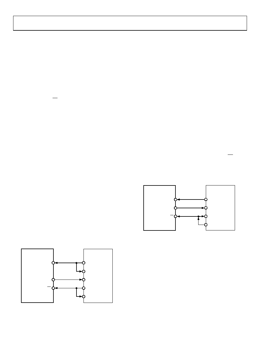
Figure 25 shows the connection diagram. It should be noted
that for signal processing applications, it is imperative that the
frame synchronization signal from the TMS320C541 provides
equidistant sampling.
AD7910/AD7920*
SCLK
SDATA
CS
CLKX
CLKR
FSX
FSR
TMS320C541*
*ADDITIONAL PINS OMITTED FOR CLARITY
DR
02976-025
Figure 25. Interfacing to the TMS320C541
AD7910/AD7920 TO ADSP-218x
The ADSP-218x family of DSPs is interfaced directly to the
AD7910/AD7920 without any glue logic required. The SPORT
control register should be set up as follows:
TFSW = RFSW = 1, Alternate Framing
INVRFS = INVTFS = 1, Active Low Frame Signal
DTYPE = 00, Right Justify Data
ISCLK = 1, Internal Serial Clock
TFSR = RFSR = 1, Frame Every Word
IRFS = 0, Sets up RFS as an Input
ITFS = 1, Sets up TFS as an Output
SLEN = 1111, 16 Bits for the AD7920
SLEN = 1101, 14 Bits for the AD7910
To implement power-down mode, SLEN should be set to 0111
to issue an 8-bit SCLK burst. The connection diagram is shown
in Figure 26. The ADSP-218x has the TFS and RFS of the
SPORT tied together, with TFS set as an output and RFS set as
an input. The DSP operates in alternate framing mode and the
SPORT control register is set up as described. The frame
synchronization signal generated on the TFS is tied to CS and,
as with all signal processing applications, equidistant sampling
is necessary. However, in this example, the timer interrupt is
used to control the sampling rate of the ADC and, under certain
conditions, equidistant sampling can not be achieved.
AD7910/AD7920*
SCLK
SDATA
CS
SCLK
DR
RFS
TFS
ADSP-218x*
02976-026
*ADDITIONAL PINS OMITTED FOR CLARITY
Figure 26. Interfacing to the ADSP-218x
The timer registers are loaded with a value that provides an
interrupt at the required sample interval. When an interrupt is
received, a value is transmitted with TFS/DT (ADC control
word). The TFS is used to control the RFS and thus the reading
of data. The frequency of the serial clock is set in the SCLKDIV
register. When the instruction to transmit with TFS is given,
that is, TX0 = AX0, the state of the SCLK is checked. The DSP
waits until the SCLK has gone high, low, and high before
transmission starts. If the timer and SCLK values are chosen
such that the instruction to transmit occurs on or near the
rising edge of SCLK, the data can be transmitted or it can wait
until the next clock edge.
相关PDF资料 |
PDF描述 |
|---|---|
| VE-J5P-MX | CONVERTER MOD DC/DC 13.8V 75W |
| VI-BNR-IV-F4 | CONVERTER MOD DC/DC 7.5V 150W |
| D38999/26WB5SNLC | CONN HSG PLUG 5POS STRGHT SCKT |
| MS3106A20-25P | CONN PLUG 13POS STRAIGHT W/PINS |
| D38999/20WC4PNLC | CONN HSG RCPT 4POS WALL MT PINS |
相关代理商/技术参数 |
参数描述 |
|---|---|
| AD7920BKS | 制造商:AD 制造商全称:Analog Devices 功能描述:250 kSPS, 10-/12-Bit ADCs in 6-Lead SC70 |
| AD7920BKS-500RL7 | 制造商:Analog Devices 功能描述:ADC Single SAR 250ksps 12-bit Serial 6-Pin SC-70 T/R 制造商:Rochester Electronics LLC 功能描述:12-BIT 250KSPS,ADC SC70 PKG I.C. - Bulk |
| AD7920BKS-REEL | 制造商:AD 制造商全称:Analog Devices 功能描述:250 kSPS, 10-/12-Bit ADCs in 6-Lead SC70 |
| AD7920BKS-REEL7 | 制造商:Analog Devices 功能描述:ADC Single SAR 250ksps 12-bit Serial 6-Pin SC-70 T/R |
| AD7920BKSZ-500RL7 | 功能描述:IC ADC 12BIT SRL 250KSPS SC70-6 RoHS:是 类别:集成电路 (IC) >> 数据采集 - 模数转换器 系列:- 标准包装:1 系列:microPOWER™ 位数:8 采样率(每秒):1M 数据接口:串行,SPI? 转换器数目:1 功率耗散(最大):- 电压电源:模拟和数字 工作温度:-40°C ~ 125°C 安装类型:表面贴装 封装/外壳:24-VFQFN 裸露焊盘 供应商设备封装:24-VQFN 裸露焊盘(4x4) 包装:Digi-Reel® 输入数目和类型:8 个单端,单极 产品目录页面:892 (CN2011-ZH PDF) 其它名称:296-25851-6 |
发布紧急采购,3分钟左右您将得到回复。