- 您现在的位置:买卖IC网 > PDF目录10314 > AD7933BRU-REEL7 (Analog Devices Inc)IC ADC 10BIT 4CH 1.5MSPS 28TSSOP PDF资料下载
参数资料
| 型号: | AD7933BRU-REEL7 |
| 厂商: | Analog Devices Inc |
| 文件页数: | 8/32页 |
| 文件大小: | 0K |
| 描述: | IC ADC 10BIT 4CH 1.5MSPS 28TSSOP |
| 标准包装: | 1,000 |
| 位数: | 10 |
| 采样率(每秒): | 1.5M |
| 数据接口: | 并联 |
| 转换器数目: | 1 |
| 功率耗散(最大): | 13.5mW |
| 电压电源: | 单电源 |
| 工作温度: | -40°C ~ 85°C |
| 安装类型: | 表面贴装 |
| 封装/外壳: | 28-TSSOP(0.173",4.40mm 宽) |
| 供应商设备封装: | 28-TSSOP |
| 包装: | 带卷 (TR) |
| 输入数目和类型: | 4 个单端,单极;2 个差分,单极;2 个伪差分,单极 |
第1页第2页第3页第4页第5页第6页第7页当前第8页第9页第10页第11页第12页第13页第14页第15页第16页第17页第18页第19页第20页第21页第22页第23页第24页第25页第26页第27页第28页第29页第30页第31页第32页
AD7933/AD7934
Rev. B | Page 16 of 32
SEQUENCER OPERATION
The configuration of the SEQ0 and SEQ1 bits in the control
register allows use of the sequencer function. Table 11 outlines
the two sequencer modes of operation.
Writing to the Control Register to Program the Sequencer
The AD7933 and AD7934 need 13 full CLKIN periods to
perform a conversion. If the ADC does not receive the full 13
CLKIN periods, the conversion aborts. If a conversion is
aborted after applying 12.5 CLKIN periods to the ADC, ensure
that a rising edge of CONVST or a falling edge of CLKIN is
applied to the part before writing to the control register to
program the sequencer. If these conditions are not met, the
sequencer will not be in the correct state to handle being
reprogrammed for another sequence of conversions and the
performance of the converter is not guaranteed.
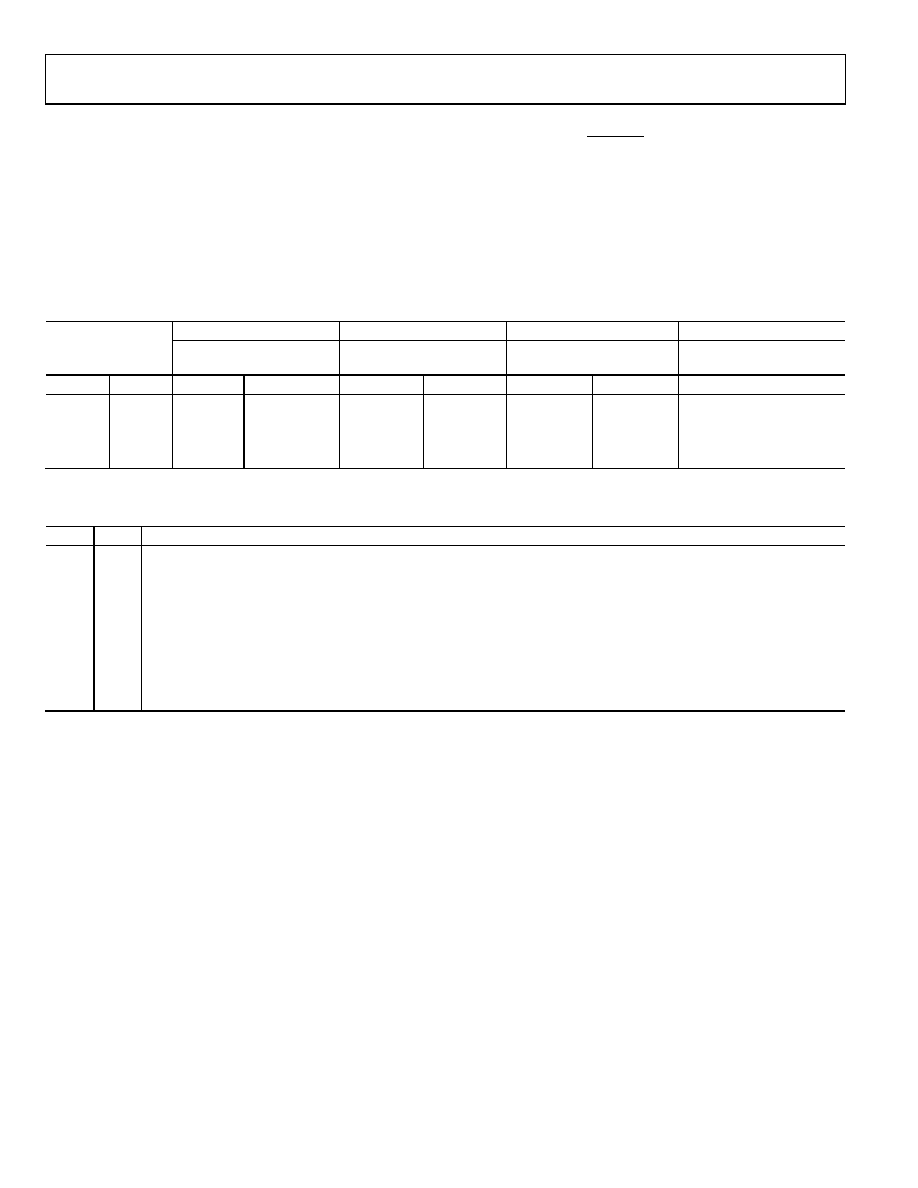
Table 10. Analog Input Type Selection
MODE0 = 0, MODE1 = 0
MODE0 = 0, MODE1 = 1
MODE0 = 1, MODE1 = 0
MODE0 = 1, MODE1 = 1
Channel Address
Four Single-Ended
Input Channels
Two Fully Differential
Input Channels
Two Pseudo Differential
Input Channels
Not Used
ADD1
ADD0
VIN+
VIN
VIN+
VIN
VIN+
VIN
0
VIN0
AGND
VIN0
VIN1
VIN0
VIN1
0
1
VIN1
AGND
VIN1
VIN0
VIN1
VIN0
1
0
VIN2
AGND
VIN2
VIN3
VIN2
VIN3
1
VIN3
AGND
VIN3
VIN2
VIN3
VIN2
Table 11. Sequence Selection Modes
SEQ0
SEQ1
Sequence Type
0
Select this configuration when the sequence function is not used. The analog input channel selected on each individual
conversion is determined by the contents of ADD1 and ADD0, the channel address bits, in each prior write operation. This
mode of operation reflects the normal operation of a multichannel ADC, without using the sequencer function, where
each write to the AD7933/AD7934 selects the next channel for conversion.
0
1
Not used.
1
0
Not used.
1
Use this configuration in conjunction with ADD1 and ADD0, the channel address bits, to program continuous conversions
on a consecutive sequence of channels. The sequence of channels extends from Channel 0 through to a selected final
channel as determined by the channel address bits in the control register. When in differential or pseudo differential mode,
inverse channels (for example, VIN1, VIN0) are not converted.
相关PDF资料 |
PDF描述 |
|---|---|
| AD7450ARZ-REEL | IC ADC 12BIT DIFF IN 1MSPS 8SOIC |
| VE-B3X-MY | CONVERTER MOD DC/DC 5.2V 50W |
| VE-B3W-MY | CONVERTER MOD DC/DC 5.5V 50W |
| VE-B3T-MY | CONVERTER MOD DC/DC 6.5V 50W |
| VE-B3R-MY | CONVERTER MOD DC/DC 7.5V 50W |
相关代理商/技术参数 |
参数描述 |
|---|---|
| AD7933BRUZ | 功能描述:IC ADC 10BIT 4CH 1.5MSPS 28TSSOP RoHS:是 类别:集成电路 (IC) >> 数据采集 - 模数转换器 系列:- 标准包装:1 系列:microPOWER™ 位数:8 采样率(每秒):1M 数据接口:串行,SPI? 转换器数目:1 功率耗散(最大):- 电压电源:模拟和数字 工作温度:-40°C ~ 125°C 安装类型:表面贴装 封装/外壳:24-VFQFN 裸露焊盘 供应商设备封装:24-VQFN 裸露焊盘(4x4) 包装:Digi-Reel® 输入数目和类型:8 个单端,单极 产品目录页面:892 (CN2011-ZH PDF) 其它名称:296-25851-6 |
| AD7933BRUZ-REEL7 | 功能描述:IC ADC 10BIT 4CH 1.5MSPS 28TSSOP RoHS:是 类别:集成电路 (IC) >> 数据采集 - 模数转换器 系列:- 标准包装:1,000 系列:- 位数:16 采样率(每秒):45k 数据接口:串行 转换器数目:2 功率耗散(最大):315mW 电压电源:模拟和数字 工作温度:0°C ~ 70°C 安装类型:表面贴装 封装/外壳:28-SOIC(0.295",7.50mm 宽) 供应商设备封装:28-SOIC W 包装:带卷 (TR) 输入数目和类型:2 个单端,单极 |
| AD7934 | 制造商:AD 制造商全称:Analog Devices 功能描述:4-Channel, 1.5 MSPS, 12-Bit and 10-Bit Parallel ADCs with a Sequencer |
| AD7934-6 | 制造商:AD 制造商全称:Analog Devices 功能描述:4-Channel, 625 kSPS, 12-Bit Parallel ADC with a Sequencer |
| AD7934BRU | 功能描述:IC ADC 12BIT 4CH 1.5MSPS 28TSSOP RoHS:否 类别:集成电路 (IC) >> 数据采集 - 模数转换器 系列:- 标准包装:1,000 系列:- 位数:12 采样率(每秒):300k 数据接口:并联 转换器数目:1 功率耗散(最大):75mW 电压电源:单电源 工作温度:0°C ~ 70°C 安装类型:表面贴装 封装/外壳:24-SOIC(0.295",7.50mm 宽) 供应商设备封装:24-SOIC 包装:带卷 (TR) 输入数目和类型:1 个单端,单极;1 个单端,双极 |
发布紧急采购,3分钟左右您将得到回复。