- 您现在的位置:买卖IC网 > PDF目录10314 > AD7933BRU-REEL7 (Analog Devices Inc)IC ADC 10BIT 4CH 1.5MSPS 28TSSOP PDF资料下载
参数资料
| 型号: | AD7933BRU-REEL7 |
| 厂商: | Analog Devices Inc |
| 文件页数: | 9/32页 |
| 文件大小: | 0K |
| 描述: | IC ADC 10BIT 4CH 1.5MSPS 28TSSOP |
| 标准包装: | 1,000 |
| 位数: | 10 |
| 采样率(每秒): | 1.5M |
| 数据接口: | 并联 |
| 转换器数目: | 1 |
| 功率耗散(最大): | 13.5mW |
| 电压电源: | 单电源 |
| 工作温度: | -40°C ~ 85°C |
| 安装类型: | 表面贴装 |
| 封装/外壳: | 28-TSSOP(0.173",4.40mm 宽) |
| 供应商设备封装: | 28-TSSOP |
| 包装: | 带卷 (TR) |
| 输入数目和类型: | 4 个单端,单极;2 个差分,单极;2 个伪差分,单极 |
第1页第2页第3页第4页第5页第6页第7页第8页当前第9页第10页第11页第12页第13页第14页第15页第16页第17页第18页第19页第20页第21页第22页第23页第24页第25页第26页第27页第28页第29页第30页第31页第32页
AD7933/AD7934
Rev. B | Page 17 of 32
CIRCUIT INFORMATION
The AD7933/AD7934 are fast, 4-channel, 10-bit and 12-bit,
single-supply, successive approximation analog-to-digital
converters. The parts operate from a 2.7 V to 5.25 V power
supply and feature throughput rates up to 1.5 MSPS.
The AD7933/AD7934 provide the user with an on-chip
track-and-hold, an internal accurate reference, an analog-to-
digital converter, and a parallel interface housed in a 28-lead
TSSOP package.
The AD7933/AD7934 have four analog input channels that
can be configured to be four single-ended inputs, two fully
differential pairs, or two pseudo differential pairs. There is
an on-chip channel sequencer that allows the user to select a
consecutive sequence of channels through which the ADC can
cycle with each falling edge of CONVST.
The analog input range for the AD7933/AD7934 is 0 V to VREF
or 0 V to 2 × VREF, depending on the status of the RANGE bit in
the control register. The output coding of the ADC can be either
binary or twos complement, depending on the status of the
CODING bit in the control register.
The AD7933/AD7934 provide flexible power management
options to allow users to achieve the best power performance
for a given throughput rate. These options are selected by
programming PM1 and PM0, the power management bits, in
the control register.
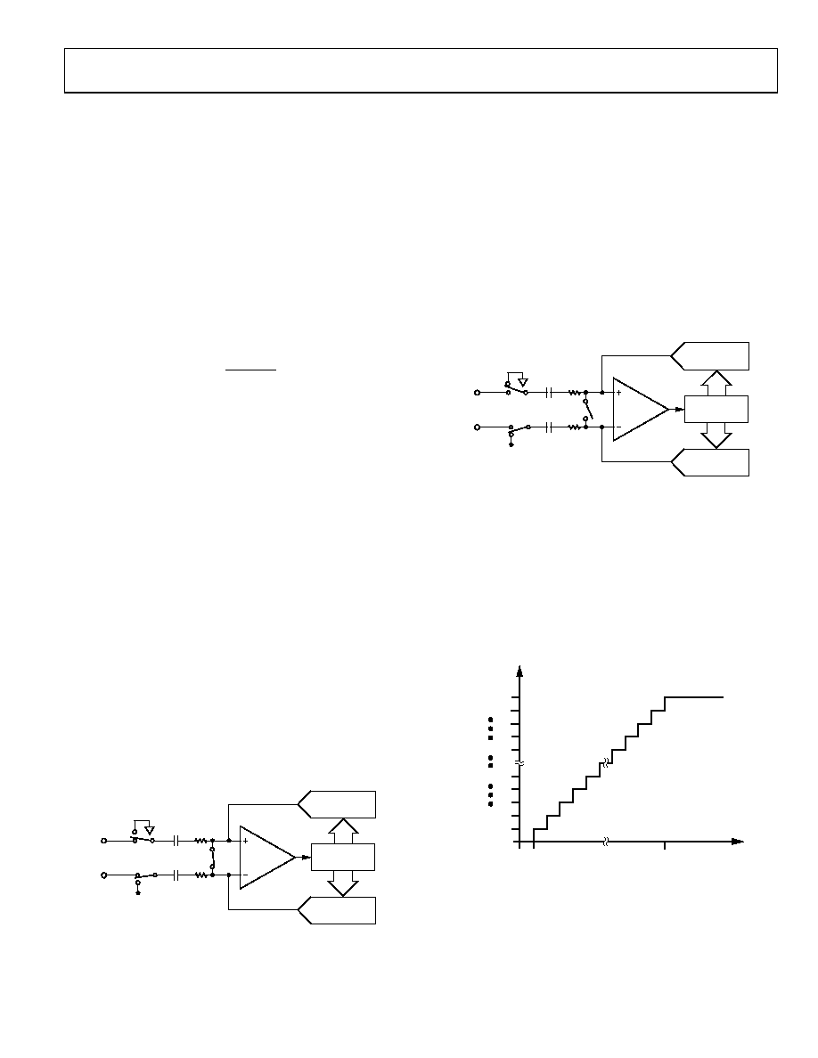
CONVERTER OPERATION
The AD7933/AD7934 are successive approximation ADCs
based around two capacitive digital-to-analog converters (DACs).
in acquisition and conversion phase, respectively. The ADC
comprises control logic, a SAR, and two capacitive DACs. Both
figures show the operation of the ADC in differential/pseudo
differential modes. Single-ended mode operation is similar but
VIN is internally tied to AGND. In acquisition phase, SW3 is
closed, SW1 and SW2 are in Position A, the comparator is held
in a balanced condition, and the sampling capacitor arrays
acquire the differential signal on the input.
VIN+
VIN–
A
B
SW1
SW3
COMPARATOR
CONTROL
LOGIC
CAPACITIVE
DAC
CAPACITIVE
DAC
CS
VREF
SW2
B
A
037
13
-02
3
Figure 14. ADC Acquisition Phase
When the ADC starts a conversion (see Figure 15), SW3 opens
and SW1 and SW2 move to Position B, causing the comparator
to become unbalanced. Both inputs are disconnected once the
conversion begins. The control logic and charge redistribution
DACs are used to add and subtract fixed amounts of charge
from the sampling capacitor arrays to bring the comparator
back into a balanced condition. When the comparator is
rebalanced, the conversion is complete. The control logic
generates the output code of the ADC. The output impedances
of the sources driving the VIN+ and the VIN pins must match;
otherwise, the two inputs have different settling times, resulting
in errors.
VIN+
VIN–
A
B
SW1
SW3
COMPARATOR
CONTROL
LOGIC
CAPACITIVE
DAC
CAPACITIVE
DAC
CS
VREF
SW2
B
A
03
713
-02
4
Figure 15. ADC Conversion Phase
ADC TRANSFER FUNCTION
The output coding for the AD7933/AD7934 is either straight
binary or twos complement, depending on the status of the
CODING bit in the control register. The designed code transitions
occur at successive LSB values (1 LSB, 2 LSBs, and so on), and
the LSB size is VREF/1024 for the AD7933 and VREF/4096 for the
AD7934. The ideal transfer characteristics of the AD7933/AD7934
for both straight binary and twos complement output coding are
000...000
111...111
1LSB = VREF/4096 (AD7934)
1LSB = VREF/1024 (AD7933)
1LSB
+VREF –1 LSB
ANALOG INPUT
A
DC
CO
DE
0V
NOTES
1. VREF IS EITHER VREF OR 2 × VREF.
000...001
000...010
111...110
111...000
011...111
03
71
3-
0
25
Figure 16. AD7933/AD7934 Ideal Transfer Characteristic
with Straight Binary Output Coding
相关PDF资料 |
PDF描述 |
|---|---|
| AD7450ARZ-REEL | IC ADC 12BIT DIFF IN 1MSPS 8SOIC |
| VE-B3X-MY | CONVERTER MOD DC/DC 5.2V 50W |
| VE-B3W-MY | CONVERTER MOD DC/DC 5.5V 50W |
| VE-B3T-MY | CONVERTER MOD DC/DC 6.5V 50W |
| VE-B3R-MY | CONVERTER MOD DC/DC 7.5V 50W |
相关代理商/技术参数 |
参数描述 |
|---|---|
| AD7933BRUZ | 功能描述:IC ADC 10BIT 4CH 1.5MSPS 28TSSOP RoHS:是 类别:集成电路 (IC) >> 数据采集 - 模数转换器 系列:- 标准包装:1 系列:microPOWER™ 位数:8 采样率(每秒):1M 数据接口:串行,SPI? 转换器数目:1 功率耗散(最大):- 电压电源:模拟和数字 工作温度:-40°C ~ 125°C 安装类型:表面贴装 封装/外壳:24-VFQFN 裸露焊盘 供应商设备封装:24-VQFN 裸露焊盘(4x4) 包装:Digi-Reel® 输入数目和类型:8 个单端,单极 产品目录页面:892 (CN2011-ZH PDF) 其它名称:296-25851-6 |
| AD7933BRUZ-REEL7 | 功能描述:IC ADC 10BIT 4CH 1.5MSPS 28TSSOP RoHS:是 类别:集成电路 (IC) >> 数据采集 - 模数转换器 系列:- 标准包装:1,000 系列:- 位数:16 采样率(每秒):45k 数据接口:串行 转换器数目:2 功率耗散(最大):315mW 电压电源:模拟和数字 工作温度:0°C ~ 70°C 安装类型:表面贴装 封装/外壳:28-SOIC(0.295",7.50mm 宽) 供应商设备封装:28-SOIC W 包装:带卷 (TR) 输入数目和类型:2 个单端,单极 |
| AD7934 | 制造商:AD 制造商全称:Analog Devices 功能描述:4-Channel, 1.5 MSPS, 12-Bit and 10-Bit Parallel ADCs with a Sequencer |
| AD7934-6 | 制造商:AD 制造商全称:Analog Devices 功能描述:4-Channel, 625 kSPS, 12-Bit Parallel ADC with a Sequencer |
| AD7934BRU | 功能描述:IC ADC 12BIT 4CH 1.5MSPS 28TSSOP RoHS:否 类别:集成电路 (IC) >> 数据采集 - 模数转换器 系列:- 标准包装:1,000 系列:- 位数:12 采样率(每秒):300k 数据接口:并联 转换器数目:1 功率耗散(最大):75mW 电压电源:单电源 工作温度:0°C ~ 70°C 安装类型:表面贴装 封装/外壳:24-SOIC(0.295",7.50mm 宽) 供应商设备封装:24-SOIC 包装:带卷 (TR) 输入数目和类型:1 个单端,单极;1 个单端,双极 |
发布紧急采购,3分钟左右您将得到回复。