- 您现在的位置:买卖IC网 > PDF目录17070 > AD7940-DBRD (Analog Devices Inc)BOARD EVAL FOR AD7940 STAMP SPI PDF资料下载
参数资料
| 型号: | AD7940-DBRD |
| 厂商: | Analog Devices Inc |
| 文件页数: | 16/20页 |
| 文件大小: | 0K |
| 描述: | BOARD EVAL FOR AD7940 STAMP SPI |
| 标准包装: | 1 |
| ADC 的数量: | 1 |
| 位数: | 14 |
| 采样率(每秒): | 100k |
| 数据接口: | 串行 |
| 输入范围: | 0 ~ Vdd |
| 在以下条件下的电源(标准): | 17mW @ 100kSPS & 5V |
| 工作温度: | -40°C ~ 85°C |
| 已用 IC / 零件: | AD7940 |
| 已供物品: | 板 |
| 相关产品: | AD7940BRJZ-REEL7DKR-ND - IC ADC 14BIT 100KSPS SOT-23-6 AD7940BRJZ-REEL7CT-ND - IC ADC 14BIT 100KSPS SOT-23-6 AD7940BRJZ-REEL7TR-ND - IC ADC 14BIT 100KSPS SOT-23-6 AD7940BRM-ND - IC ADC 14BIT UNIPOLAR 8-MSOP AD7940BRM-REEL7TR-ND - IC ADC 14BIT UNIPOLAR 8-MSOP |
AD7940
Rev. A | Page 5 of 20
TIMING SPECIFICATIONS
Sample tested at initial release to ensure compliance. All input signals are specified with tr = tf = 5 ns (10% to 90% of VDD) and timed from
a voltage level of 1.6 V.
VDD = 2.50 V to 5.5 V; TA = TMIN to TMAX, unless otherwise noted.
Table 3.
Limit at T
MIN, TMAX
Parameter
3 V
5 V
Unit
Description
f
SCLK
250
kHz min
2.5
MHz max
t
CONVERT
16 × t
SCLK
16 × t
SCLK
min
t
QUIET
50
ns min
Minimum quiet time required between bus relinquish and start of
next conversion
t
1
10
ns min
Minimum CS pulse width
t
2
10
ns min
CS to SCLK setup time
t
3
48
35
ns max
Delay from CS until SDATA three-state disabled
t
4
2
120
80
ns max
Data access time after SCLK falling edge
t
5
0.4 t
SCLK
0.4 t
SCLK
ns min
SCLK low pulse width
t
6
0.4 t
SCLK
0.4 t
SCLK
ns min
SCLK high pulse width
t
7
10
ns min
SCLK to data valid hold time
t
8
45
35
ns max
SCLK falling edge to SDATA high impedance
t
POWER-UP
1
s typ
Power up time from full power-down
1 Mark/space ratio for the SCLK input is 40/60 to 60/40.
2 Measured with the load circuit of Figure 2 and defined as the time required for the output to cross 0.8 V or 2.0 V.
3 t
8 is derived form the measured time taken by the data outputs to change 0.5 V when loaded with the circuit of Figure 2. The measured number is then extrapolated
back to remove the effects of charging or discharging the 50 pF capacitor. This means that the time, t8, quoted in the timing characteristics is the true bus relinquish
time of the part and is independent of the bus loading.
4 See the Power vs. Throughput Rate section.
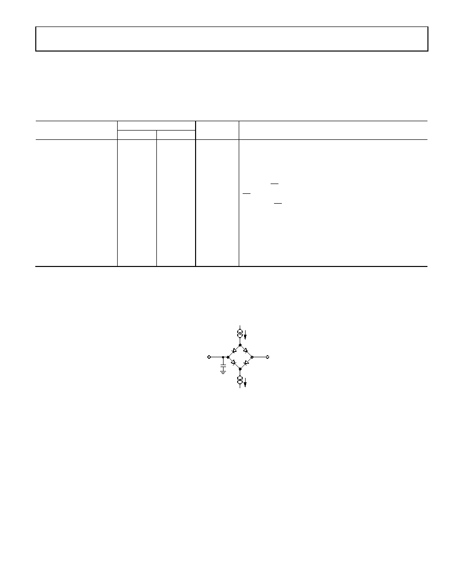
03305-0-002
200
A
IOL
200
A
IOH
1.6V
TO OUTPUT
PIN
CL
50pF
Figure 2. Load Circuit for Digital Output Timing Specification
相关PDF资料 |
PDF描述 |
|---|---|
| EVAL-AD5663REBZ | BOARD EVAL FOR AD5663 |
| NRS6010T3R3MMGF | INDUCTOR POWER 3.3UH 1.5A SMD |
| EVAL-AD5390EBZ | BOARD EVALUATION FOR AD5390 |
| MIC2026-1YM TR | IC SW DISTRIBUTION 2CHAN 8SOIC |
| EVAL-AD5680EBZ | BOARD EVAL FOR AD5680 |
相关代理商/技术参数 |
参数描述 |
|---|---|
| AD7942 | 制造商:AD 制造商全称:Analog Devices 功能描述:16-Bit, +/-0.65 LSB INL, 500 kSPS PulSAR Differential ADC in MSOP/QFN |
| AD79421 | 制造商:AD 制造商全称:Analog Devices 功能描述:18-Bit, 2 MSPS PulSAR 15 mW ADC in LFCSP (QFN) |
| AD7942BCPRL7 | 制造商:AD 制造商全称:Analog Devices 功能描述:14-Bit, 250 kSPS PulSAR ADC in MSOP/QFN |
| AD7942BCPWP | 制造商:AD 制造商全称:Analog Devices 功能描述:14-Bit, 250 kSPS PulSAR ADC in MSOP/QFN |
| AD7942BCPZRL | 功能描述:IC ADC 14BIT SAR 250KSPS 10LFCSP RoHS:是 类别:集成电路 (IC) >> 数据采集 - 模数转换器 系列:PulSAR® 标准包装:1,000 系列:- 位数:16 采样率(每秒):45k 数据接口:串行 转换器数目:2 功率耗散(最大):315mW 电压电源:模拟和数字 工作温度:0°C ~ 70°C 安装类型:表面贴装 封装/外壳:28-SOIC(0.295",7.50mm 宽) 供应商设备封装:28-SOIC W 包装:带卷 (TR) 输入数目和类型:2 个单端,单极 |
发布紧急采购,3分钟左右您将得到回复。