参数资料
| 型号: | AD7983BCPZ-RL7 |
| 厂商: | Analog Devices Inc |
| 文件页数: | 22/24页 |
| 文件大小: | 0K |
| 描述: | IC ADC 16BIT 1.33MSPS 10LFCSP |
| 标准包装: | 1 |
| 系列: | PulSAR® |
| 位数: | 16 |
| 采样率(每秒): | 1.33M |
| 数据接口: | DSP,MICROWIRE?,QSPI?,串行,SPI? |
| 转换器数目: | 1 |
| 功率耗散(最大): | 12mW |
| 电压电源: | 单电源 |
| 工作温度: | -40°C ~ 85°C |
| 安装类型: | 表面贴装 |
| 封装/外壳: | 10-WFDFN 裸露焊盘,CSP |
| 供应商设备封装: | 10-LFCSP-WD(3x3) |
| 包装: | 标准包装 |
| 输入数目和类型: | 1 个差分,单极 |
| 其它名称: | AD7983BCPZ-RL7DKR |
AD7983
Rev. A | Page 7 of 24
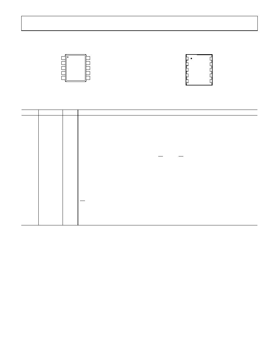
PIN CONFIGURATIONS AND FUNCTION DESCRIPTIONS
REF 1
VDD 2
IN+ 3
IN– 4
VIO
10
SDI
9
SCK
8
SDO
7
GND 5
CNV
6
06
97
4
-00
4
AD7983
TOP VIEW
(Not to Scale)
Figure 4. 10-Lead MSOP Pin Configuration
REF 1
10 VIO
VDD 2
9 SDI
IN+ 3
8 SCK
IN– 4
7 SDO
6 CNV
AD7983
TOP VIEW
(Not to Scale)
06
97
4-
00
5
GND 5
Figure 5. 10-Lead QFN (LFCSP) Pin Configuration
Table 6. Pin Function Descriptions
Pin No.
Mnemonic
Description
1
REF
AI
Reference Input Voltage. The REF range is from 2.9 V to 5.1 V. It is referred to the GND pin. This pin should
be decoupled closely to the pin with a 10 μF capacitor.
2
VDD
P
Power Supply.
3
IN+
AI
Analog Input. It is referred to IN. The voltage range, for example, the difference between IN+ and IN, is
0 V to VREF.
4
IN
AI
Analog Input Ground Sense. To be connected to the analog ground plane or to a remote sense ground.
5
GND
P
Power Supply Ground.
6
CNV
DI
Convert Input. This input has multiple functions. On its risng edge, it initiates the conversions and
selects the interface mode of the part: chain or CS mode. In CS mode, it enables the SDO pin when low.
In chain mode, the data should be read when CNV is high.
7
SDO
DO
Serial Data Output. The conversion result is output on this pin. It is synchronized to SCK.
8
SCK
DI
Serial Data Clock Input. When the part is selected, the conversion result is shifted out by this clock.
9
SDI
DI
Serial Data Input. This input provides multiple features. It selects the interface mode of the ADC as
follows:
Chain mode is selected if SDI is low during the CNV rising edge. In this mode, SDI is used as a data
input to daisy-chain the conversion results of two or more ADCs onto a single SDO line. The digital
data level on SDI is output on SDO with a delay of 16 SCK cycles.
CS mode is selected if SDI is high during the CNV rising edge. In this mode, either SDI or CNV can
enable the serial output signals when low; if SDI or CNV is low when the conversion is complete,
the busy indicator feature is enabled.
10
VIO
P
Input/Output Interface Digital Power. Nominally at the same supply as the host interface (1.8 V, 2.5 V,
3 V, or 5 V).
1 AI = analog input, DI = digital input, DO = digital output, and P = power.
相关PDF资料 |
PDF描述 |
|---|---|
| AD7984BCPZ-RL7 | IC ADC 18BIT 1.33MSPS 10LFCSP |
| AD7985BCPZ-RL7 | IC ADC 16B 2.5MSPS PULSR 20LFCSP |
| AD7986BCPZ-RL7 | IC ADC 18BIT 2MSPS SAR 20LFCSP |
| AD7988-1BRMZ-RL7 | IC ADC 16BIT SRL 100KSPS 10MSOP |
| AD7991YRJZ-1RL | IC ADC 12BIT 4CH I2C SOT23-8 |
相关代理商/技术参数 |
参数描述 |
|---|---|
| AD7983BRMZ | 功能描述:IC ADC 16BIT 1.33MSPS 10MSOP RoHS:是 类别:集成电路 (IC) >> 数据采集 - 模数转换器 系列:PulSAR® 标准包装:1 系列:microPOWER™ 位数:8 采样率(每秒):1M 数据接口:串行,SPI? 转换器数目:1 功率耗散(最大):- 电压电源:模拟和数字 工作温度:-40°C ~ 125°C 安装类型:表面贴装 封装/外壳:24-VFQFN 裸露焊盘 供应商设备封装:24-VQFN 裸露焊盘(4x4) 包装:Digi-Reel® 输入数目和类型:8 个单端,单极 产品目录页面:892 (CN2011-ZH PDF) 其它名称:296-25851-6 |
| AD7983BRMZRL7 | 制造商:AD 制造商全称:Analog Devices 功能描述:16-Bit, 1.33 MSPS PulSAR ADC in MSOP/QFN |
| AD7983BRMZ-RL7 | 功能描述:IC ADC 16BIT 1.33MSPS 10MSOP RoHS:是 类别:集成电路 (IC) >> 数据采集 - 模数转换器 系列:PulSAR® 标准包装:1 系列:- 位数:14 采样率(每秒):83k 数据接口:串行,并联 转换器数目:1 功率耗散(最大):95mW 电压电源:双 ± 工作温度:0°C ~ 70°C 安装类型:通孔 封装/外壳:28-DIP(0.600",15.24mm) 供应商设备封装:28-PDIP 包装:管件 输入数目和类型:1 个单端,双极 |
| AD7984 | 制造商:AD 制造商全称:Analog Devices 功能描述:18-Bit, 1.33 MSPS PulSAR 10.5 mW ADC in MSOP/QFN |
| AD79841 | 制造商:AD 制造商全称:Analog Devices 功能描述:18-Bit, 2 MSPS PulSAR 15 mW ADC in LFCSP (QFN) |
发布紧急采购,3分钟左右您将得到回复。