- 您现在的位置:买卖IC网 > PDF目录10659 > AD7983BRMZ (Analog Devices Inc)IC ADC 16BIT 1.33MSPS 10MSOP PDF资料下载
参数资料
| 型号: | AD7983BRMZ |
| 厂商: | Analog Devices Inc |
| 文件页数: | 15/24页 |
| 文件大小: | 0K |
| 描述: | IC ADC 16BIT 1.33MSPS 10MSOP |
| 标准包装: | 1 |
| 系列: | PulSAR® |
| 位数: | 16 |
| 采样率(每秒): | 1.33M |
| 数据接口: | DSP,MICROWIRE?,QSPI?,串行,SPI? |
| 转换器数目: | 1 |
| 功率耗散(最大): | 12mW |
| 电压电源: | 单电源 |
| 工作温度: | -40°C ~ 85°C |
| 安装类型: | 表面贴装 |
| 封装/外壳: | 10-TFSOP,10-MSOP(0.118",3.00mm 宽) |
| 供应商设备封装: | 10-MSOP |
| 包装: | 管件 |
| 输入数目和类型: | 1 个差分,单极 |
| 产品目录页面: | 780 (CN2011-ZH PDF) |
AD7983
Rev. A | Page 22 of 24
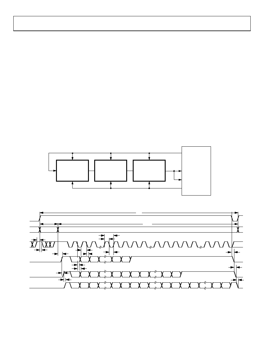
CHAIN MODE WITH BUSY INDICATOR
This mode can also be used to daisy-chain multiple AD7983s
on a 3-wire serial interface while providing a busy indicator.
This feature is useful for reducing component count and wiring
connections, for example, in isolated multiconverter applications or
for systems with a limited interfacing capacity. Data readback is
analogous to clocking a shift register.
A connection diagram example using three AD7983s is shown
in Figure 36, and the corresponding timing is given in Figure 37.
When SDI and CNV are low, SDO is driven low. With SCK
high, a rising edge on CNV initiates a conversion, selects the
chain mode, and enables the busy indicator feature. In this
mode, CNV is held high during the conversion phase and the
subsequent data readback. When all ADCs in the chain have
completed their conversions, the SDO pin of the ADC closest
to the digital host (see the AD7983 ADC labeled C in Figure 36)
is driven high. This transition on SDO can be used as a busy
indicator to trigger the data readback controlled by the digital
host. The AD7983 then enters the acquisition phase and goes
into standby mode. The data bits stored in the internal shift
register are clocked out, MSB first, by subsequent SCK falling
edges. For each ADC, SDI feeds the input of the internal shift
register and is clocked by the SCK falling edge. Each ADC in the
chain outputs its data MSB first, and 16 × N + 1 clocks are required
to readback the N ADCs. Although the rising edge can be used
to capture the data, a digital host using the SCK falling edge
allows a faster reading rate and, consequently, more AD7983s in
the chain, provided the digital host has an acceptable hold time.
AD7983
C
SDO
SDI
DATA IN
IRQ
DIGITAL HOST
CONVERT
CLK
CNV
SCK
AD7983
B
SDO
SDI
CNV
SCK
AD7983
A
SDO
SDI
CNV
SCK
06
97
4-
02
2
Figure 36. Chain Mode with Busy Indicator Connection Diagram
tCONV
tCYC
tSSDISCK
tSCKH
tSCK
tHSDISCK
tACQ
tDSDOSDI
tDSDODSI
ACQUISITION
tSSCKCNV
ACQUISITION
tSCKL
CONVERSION
tHSCKCNV
SCK
CNV = SDIA
SDOA = SDIB
SDOB = SDIC
SDOC
tEN
DA15
DA14
DA13
DB15
DB14
DB13
DC15
DC14
DC13
DB1DB0DA15
DA14
DA1DA0
DC1DC0DB15
DB14
DA0
DA1
DB0
DB1DA14
DA15
DA1DA0
tHSDO
12
3
15
16
17
4
18
19
31
32
333435
47
48
49
tDSDO
tDSDOSDI
0697
4-
023
Figure 37. Chain Mode with Busy Indicator Serial Interface Timing
相关PDF资料 |
PDF描述 |
|---|---|
| MAX3362EKA#TG16 | IC TXRX RS485/422 SGL SOT23-8 |
| VI-J1L-MW-F3 | CONVERTER MOD DC/DC 28V 100W |
| AD1674ARZ | IC ADC 12BIT 100KSPS 28-SOIC |
| AD7693BRMZ | IC ADC 16BIT 500KSPS 10-MSOP |
| VI-J1L-MW-F2 | CONVERTER MOD DC/DC 28V 100W |
相关代理商/技术参数 |
参数描述 |
|---|---|
| AD7983BRMZRL7 | 制造商:AD 制造商全称:Analog Devices 功能描述:16-Bit, 1.33 MSPS PulSAR ADC in MSOP/QFN |
| AD7983BRMZ-RL7 | 功能描述:IC ADC 16BIT 1.33MSPS 10MSOP RoHS:是 类别:集成电路 (IC) >> 数据采集 - 模数转换器 系列:PulSAR® 标准包装:1 系列:- 位数:14 采样率(每秒):83k 数据接口:串行,并联 转换器数目:1 功率耗散(最大):95mW 电压电源:双 ± 工作温度:0°C ~ 70°C 安装类型:通孔 封装/外壳:28-DIP(0.600",15.24mm) 供应商设备封装:28-PDIP 包装:管件 输入数目和类型:1 个单端,双极 |
| AD7984 | 制造商:AD 制造商全称:Analog Devices 功能描述:18-Bit, 1.33 MSPS PulSAR 10.5 mW ADC in MSOP/QFN |
| AD79841 | 制造商:AD 制造商全称:Analog Devices 功能描述:18-Bit, 2 MSPS PulSAR 15 mW ADC in LFCSP (QFN) |
| AD7984BCPZ | 制造商:AD 制造商全称:Analog Devices 功能描述:18-Bit, 1.33 MSPS PulSAR 10.5 mW ADC in MSOP/QFN |
发布紧急采购,3分钟左右您将得到回复。