参数资料
| 型号: | AD8013ANZ |
| 厂商: | Analog Devices Inc |
| 文件页数: | 6/12页 |
| 文件大小: | 0K |
| 描述: | IC OPAMP SINGLE 14DIP |
| 标准包装: | 25 |
| 应用: | 电流反馈 |
| 电路数: | 3 |
| -3db带宽: | 140MHz |
| 转换速率: | 1000 V/µs |
| 电流 - 电源: | 3.5mA |
| 电流 - 输出 / 通道: | 30mA |
| 电压 - 电源,单路/双路(±): | 4.2 V ~ 13 V,±2.1 V ~ 6.5 V |
| 安装类型: | 通孔 |
| 封装/外壳: | 14-DIP(0.300",7.62mm) |
| 供应商设备封装: | 14-PDIP |
| 包装: | 管件 |
AD8013
Model
AD8013A
Conditions
VS
Min
Typ
Max
Units
POWER SUPPLY
Operating Range
Single Supply
+4.2
+13
V
Dual Supply
±2.1
±6.5
V
Quiescent Current/Amplifier
+5 V
3.0
3.5
mA
±5 V
3.4
4.0
mA
±6.5 V
3.5
mA
Quiescent Current/Amplifier
Power Down
+5 V
0.25
0.35
mA
±5 V
0.3
0.4
mA
Power Supply Rejection Ratio
Input Offset Voltage
VS =
±2.5 V to ±5 V
70
76
dB
–Input Current
+5 V,
±5 V
0.03
0.2
A/V
+Input Current
+5 V,
±5 V
0.07
1.0
A/V
DISABLE CHARACTERISTICS
Off Isolation
f = 6 MHz
+5 V,
±5 V
–70
dB
Off Output Impedance
G = +1
+5 V,
±5 V
12
pF
Turn-On Time
50
ns
Turn-Off Time
30
ns
Switching Threshold
–VS + xV
1.3
1.6
1.9
V
NOTES
1The test circuit for differential gain and phase measurements on a +5 V supply is ac coupled.
Specifications subject to change without notice.
–3–
REV. A
ABSOLUTE MAXIMUM RATINGS
1
Supply Voltage
. . . . . . . . . . . . . . . . . . . . . . . . . . 13.2 V Total
Internal Power Dissipation
2
Plastic (N) . . . . . . . . . 1.6 Watts (Observe Derating Curves)
Small Outline (R) . . . . 1.0 Watts (Observe Derating Curves)
Input Voltage (Common Mode) . . Lower of
±V
S or
±12.25 V
Differential Input Voltage . . . . . . . . Output
±6 V (Clamped)
Output Voltage Limit
Maximum . . . . . . . . . Lower of (+12 V from –VS) or (+VS)
Minimum . . . . . . . . . Higher of (–12.5 V from +VS) or (–VS)
Output Short Circuit Duration
. . . . . . . . . . . . . . . . . . . . Observe Power Derating Curves
Storage Temperature Range
N and R Package . . . . . . . . . . . . . . . . . . . –65
°C to +125°C
Operating Temperature Range
AD8013A . . . . . . . . . . . . . . . . . . . . . . . . . . –40
°C to +85°C
Lead Temperature Range (Soldering 10 sec) . . . . . . . . +300
°C
NOTES
1Stresses above those listed under “Absolute Maximum Ratings” may cause
permanent damage to the device. This is a stress rating only and functional
operation of the device at these or any other conditions above those indicated in
the operational section of this specification is not implied. Exposure to absolute
maximum rating conditions for extended periods may affect device reliability.
2Specification is for device in free air:
14-Pin Plastic DIP Package:
θ
JA = 75°C/Watt
14-Pin SOIC Package:
θ
JA = 120°C/Watt
ORDERING GUIDE
Temperature
Package
Model
Range
Description
Options
AD8013AN
–40
°C to +85°C 14-Pin Plastic DIP N-14
AD8013AR-14
–40
°C to +85°C 14-Pin Plastic SOIC R-14
AD8013AR-14-REEL
–40
°C to +85°C 14-Pin Plastic SOIC R-14
AD8013AR-14-REEL7
–40
°C to +85°C 14-Pin Plastic SOIC R-14
AD8013ACHIPS
–40
°C to +85°C Die Form
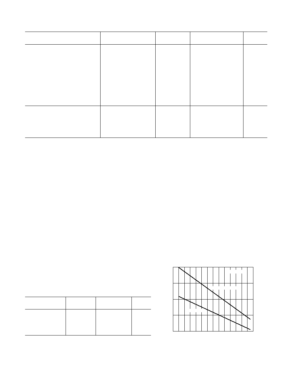
Maximum Power Dissipation
The maximum power that can be safely dissipated by the AD8013
is limited by the associated rise in junction temperature. The
maximum safe junction temperature for the plastic encapsulated
parts is determined by the glass transition temperature of the
plastic, about 150
°C. Exceeding this limit temporarily may
cause a shift in parametric performance due to a change in the
stresses exerted on the die by the package. Exceeding a junction
temperature of 175
°C for an extended period can result in
device failure.
While the AD8013 is internally short circuit protected, this may
not be enough to guarantee that the maximum junction temper-
ature is not exceeded under all conditions. To ensure proper
operation, it is important to observe the derating curves.
It must also be noted that in (noninverting) gain configurations
(with low values of gain resistor), a high level of input overdrive
can result in a large input error current, which may result in a
significant power dissipation in the input stage. This power
must be included when computing the junction temperature rise
due to total internal power.
MAXIMUM
POWER
DISSIPATION
–
Watts
AMBIENT TEMPERATURE –
°C
2.5
2.0
0.5
–50
90
–40 –30 –20
0
10 20
30
40 50
60 70
80
1.5
1.0
–10
TJ = +150°C
14-PIN DIP PACKAGE
14-PIN SOIC
Maximum Power Dissipation vs. Ambient Temperature
相关PDF资料 |
PDF描述 |
|---|---|
| AD8023ARZ | IC AMP VIDEO TRIPLE HC 14-SOIC |
| AD8073JNZ | IC VIDEO AMP TRIPLE 14-DIP |
| AD8074ARU | IC TRPL VID BUFF 500MHZ 16-TSSOP |
| AD810AN | IC CURR-FDBK AMP VIDEO LP 8-DIP |
| AD811AR-16 | IC CURR-FDBK AMP VIDEO HS 16SOIC |
相关代理商/技术参数 |
参数描述 |
|---|---|
| AD8013AR-14 | 功能描述:IC OPAMP SINGLE SUPPLY 14-SOIC RoHS:否 类别:集成电路 (IC) >> 线性 - 放大器 - 视频放大器和频缓冲器 系列:- 标准包装:1,000 系列:- 应用:驱动器 输出类型:差分 电路数:3 -3db带宽:350MHz 转换速率:1000 V/µs 电流 - 电源:14.5mA 电流 - 输出 / 通道:60mA 电压 - 电源,单路/双路(±):5 V ~ 12 V,±2.5 V ~ 6 V 安装类型:表面贴装 封装/外壳:20-VFQFN 裸露焊盘 供应商设备封装:20-QFN 裸露焊盘(4x4) 包装:带卷 (TR) |
| AD8013AR-14-EBZ | 功能描述:BOARD EVAL FOR AD8013AR-14 RoHS:是 类别:编程器,开发系统 >> 评估板 - 运算放大器 系列:- 产品培训模块:Lead (SnPb) Finish for COTS Obsolescence Mitigation Program 标准包装:1 系列:- |
| AD8013AR-14-REEL | 制造商:Analog Devices 功能描述:OP Amp Triple Current Fdbk 制造商:Rochester Electronics LLC 功能描述:TRPL LO PWR VIDEO OP AMP - Tape and Reel |
| AD8013AR-14-REEL7 | 制造商:Analog Devices 功能描述:OP Amp Triple Current Fdbk ±6.5V/13V 14-Pin SOIC N T/R 制造商:Rochester Electronics LLC 功能描述:TRPL LO PWR VIDEO OP AMP - Tape and Reel |
| AD8013ARZ-14 | 功能描述:IC AMP VIDEO SGL SUPP LP 14-SOIC RoHS:是 类别:集成电路 (IC) >> 线性 - 放大器 - 视频放大器和频缓冲器 系列:- 产品培训模块:Lead (SnPb) Finish for COTS Obsolescence Mitigation Program 标准包装:50 系列:- 应用:TFT-LCD 面板:VCOM 驱动器 输出类型:满摆幅 电路数:1 -3db带宽:35MHz 转换速率:40 V/µs 电流 - 电源:3.7mA 电流 - 输出 / 通道:1.3A 电压 - 电源,单路/双路(±):9 V ~ 20 V,±4.5 V ~ 10 V 安装类型:表面贴装 封装/外壳:8-TSSOP,8-MSOP(0.118",3.00mm 宽)裸露焊盘 供应商设备封装:8-uMax-EP 包装:管件 |
发布紧急采购,3分钟左右您将得到回复。