- 您现在的位置:买卖IC网 > PDF目录16959 > AD8065ART-EBZ (Analog Devices Inc)BOARD EVAL FOR AD8065ART PDF资料下载
参数资料
| 型号: | AD8065ART-EBZ |
| 厂商: | Analog Devices Inc |
| 文件页数: | 2/29页 |
| 文件大小: | 0K |
| 描述: | BOARD EVAL FOR AD8065ART |
| 标准包装: | 1 |
| 每 IC 通道数: | 1 - 单 |
| 放大器类型: | 电压反馈 |
| 板类型: | 裸(未填充) |
| 已供物品: | 板 |
| 已用 IC / 零件: | SOT-23-5 封装 |
第1页当前第2页第3页第4页第5页第6页第7页第8页第9页第10页第11页第12页第13页第14页第15页第16页第17页第18页第19页第20页第21页第22页第23页第24页第25页第26页第27页第28页第29页
AD8065/AD8066
Rev. J | Page 9 of 28
ABSOLUTE MAXIMUM RATINGS
RMS output voltages should be considered. If RL is referenced to
VS, as in single-supply operation, then the total drive power is
VS × IOUT.
Table 4.
Parameter
Rating
Supply Voltage
26.4 V
Power Dissipation
See Figure 3
Common-Mode Input Voltage
VEE 0.5 V to VCC + 0.5 V
Differential Input Voltage
1.8 V
Storage Temperature Range
65°C to +125°C
Operating Temperature Range
40°C to +85°C
AD8065WARTZ Only
40°C to +105°C
Lead Temperature
(Soldering, 10 sec)
300°C
If the rms signal levels are indeterminate, then consider the
worst case, when VOUT = VS/4 for RL to midsupply.
() ()
L
S
D
R
V
I
V
P
2
4
/
+
×
=
In single-supply operation with RL referenced to VS, worst case
is VOUT = VS/2.
M
A
XIM
U
M
POWER
D
ISSIPA
TION
(
W
)
0
0.5
1.0
1.5
2.0
20
0
–40
–20
–60
40
60
80
100
AMBIENT TEMPERATURE (°C)
02916-E
-003
MSOP-8
SOIC-8
SOT-23-5
Stresses above those listed under Absolute Maximum Ratings
may cause permanent damage to the device. This is a stress
rating only; functional operation of the device at these or any
other conditions above those indicated in the operational
section of this specification is not implied. Exposure to absolute
maximum rating conditions for extended periods may affect
device reliability.
MAXIMUM POWER DISSIPATION
The maximum safe power dissipation in the AD8065/AD8066
packages is limited by the associated rise in junction temperature
(TJ) on the die. The plastic encapsulating the die locally reaches
the junction temperature. At approximately 150°C, which is the
glass transition temperature, the plastic changes its properties.
Even temporarily exceeding this temperature limit can change
the stresses that the package exerts on the die, permanently
shifting the parametric performance of the AD8065/AD8066.
Exceeding a junction temperature of 175°C for an extended
time can result in changes in the silicon devices, potentially
causing failure.
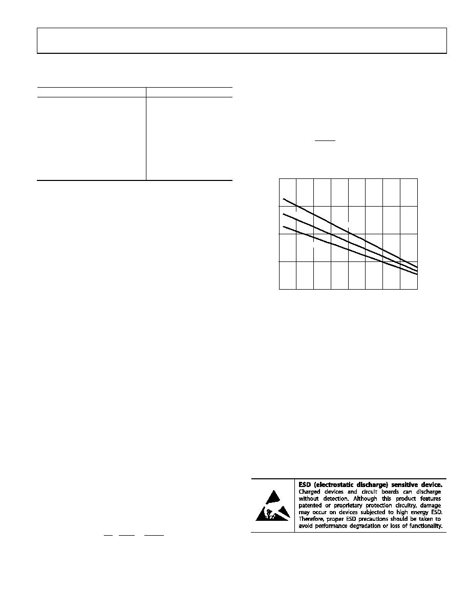
Figure 3. Maximum Power Dissipation vs. Temperature for a 4-Layer Board
Airflow increases heat dissipation, effectively reducing θJA. Also,
more metal directly in contact with the package leads from
metal traces, through holes, ground, and power planes reduce
the θJA. Care must be taken to minimize parasitic capacitances
at the input leads of high speed op amps as discussed in the
The still air thermal properties of the package and PCB (θJA),
ambient temperature (TA), and total power dissipated in the
package (PD) determine the junction temperature of the die.
The junction temperature can be calculated by
Figure 3 shows the maximum safe power dissipation in the
package vs. the ambient temperature for the SOIC (125°C/W),
SOT-23 (180°C/W), and MSOP (150°C/W) packages on a
JEDEC standard 4-layer board. θJA values are approximations.
TJ = TA + (PD × θJA)
OUTPUT SHORT CIRCUIT
The power dissipated in the package (PD) is the sum of the
quiescent power dissipation and the power dissipated in the
package due to the load drive for all outputs. The quiescent
power is the voltage between the supply pins (VS) times the
quiescent current (IS). Assuming the load (RL) is referenced to
midsupply, then the total drive power is VS /2 × IOUT, some of
which is dissipated in the package and some in the load (VOUT ×
IOUT). The difference between the total drive power and the load
power is the drive power dissipated in the package.
Shorting the output to ground or drawing excessive current for
the AD8065/AD8066 will likely cause catastrophic failure.
ESD CAUTION
(
)
Power
Load
Power
Drive
Total
Power
Quiescent
PD
+
=
()
L
OUT
L
OUT
S
D
R
V
R
V
I
V
P
2
×
+
×
=
相关PDF资料 |
PDF描述 |
|---|---|
| VE-J7Y-EY | CONVERTER MOD DC/DC 3.3V 33W |
| AD8138ARM-EBZ | BOARD EVAL FOR AD8138ARM |
| VE-J7X-EY | CONVERTER MOD DC/DC 5.2V 50W |
| AD8129AR-EBZ | BOARD EVAL FOR AD8129AR |
| RYM08DTBD | CONN EDGECARD 16POS R/A .156 SLD |
相关代理商/技术参数 |
参数描述 |
|---|---|
| AD8065ART-R2 | 制造商:Analog Devices 功能描述:OP Amp Single Volt Fdbk R-R O/P 制造商:Analog Devices 功能描述:OP Amp Single Volt Fdbk R-R O/P ±12V/24V 5-Pin SOT-23 T/R 制造商:Analog Devices 功能描述:OP AMP SGL VOLT FDBK R-R O/P 12V/24V 5PIN SOT-23 - Tape and Reel 制造商:Rochester Electronics LLC 功能描述:SOT23 HI PERF HI SPD FET AMP W/ DISABLE - Bulk 制造商:Analog Devices 功能描述:IC OP-AMP HIGH PERFORMANCE |
| AD8065ART-REEL | 功能描述:IC OPAMP VF R-R LN LP SOT23-5 RoHS:否 类别:集成电路 (IC) >> Linear - Amplifiers - Instrumentation 系列:FastFET™ 标准包装:50 系列:- 放大器类型:通用 电路数:2 输出类型:满摆幅 转换速率:1.8 V/µs 增益带宽积:6.5MHz -3db带宽:4.5MHz 电流 - 输入偏压:5nA 电压 - 输入偏移:100µV 电流 - 电源:65µA 电流 - 输出 / 通道:35mA 电压 - 电源,单路/双路(±):1.8 V ~ 5.25 V,±0.9 V ~ 2.625 V 工作温度:-40°C ~ 85°C 安装类型:表面贴装 封装/外壳:10-TFSOP,10-MSOP(0.118",3.00mm 宽) 供应商设备封装:10-MSOP 包装:管件 |
| AD8065ART-REEL7 | 功能描述:IC OPAMP VF R-R LN LP SOT23-5 RoHS:否 类别:集成电路 (IC) >> Linear - Amplifiers - Instrumentation 系列:FastFET™ 标准包装:50 系列:- 放大器类型:通用 电路数:2 输出类型:满摆幅 转换速率:1.8 V/µs 增益带宽积:6.5MHz -3db带宽:4.5MHz 电流 - 输入偏压:5nA 电压 - 输入偏移:100µV 电流 - 电源:65µA 电流 - 输出 / 通道:35mA 电压 - 电源,单路/双路(±):1.8 V ~ 5.25 V,±0.9 V ~ 2.625 V 工作温度:-40°C ~ 85°C 安装类型:表面贴装 封装/外壳:10-TFSOP,10-MSOP(0.118",3.00mm 宽) 供应商设备封装:10-MSOP 包装:管件 |
| AD8065ARTZ-R2 | 制造商:Analog Devices 功能描述:OP AMP SGL VOLT FDBK R-R O/P 12V/24V 5PIN SOT-23 - Tape and Reel 制造商:Analog Devices 功能描述:IC OP AMP SINGLE 145MHZ 5SOT23 制造商:Analog Devices 功能描述:IC OPERATIONAL AMPLIFIER SINGLE BIPOL 制造商:Analog Devices 功能描述:IC, OP AMP, SINGLE, 145MHZ, 5SOT23 制造商:Analog Devices 功能描述:OP Amp Single Volt Fdbk R-R O/P 12V/24V |
| AD8065ARTZ-R2 | 制造商:Analog Devices 功能描述:Operational Amplifier (Op-Amp) IC |
发布紧急采购,3分钟左右您将得到回复。