- 您现在的位置:买卖IC网 > PDF目录5318 > AD8065ARTZ-REEL (Analog Devices Inc)IC OPAMP VF R-R LN LP SOT23-5 PDF资料下载
参数资料
| 型号: | AD8065ARTZ-REEL |
| 厂商: | Analog Devices Inc |
| 文件页数: | 15/29页 |
| 文件大小: | 0K |
| 描述: | IC OPAMP VF R-R LN LP SOT23-5 |
| 设计资源: | Unipolar, Precision DC Digital-to-Analog Conversion Using AD5426/32/43 8-Bit to12-Bit DACs (CN0034) Programmable Gain Element Using AD5426/32/43 Current Output DACs (CN0038) Programmable Gain Element Using AD5450/1/2/3 Current Output DAC Family (CN0055) |
| 标准包装: | 10,000 |
| 系列: | FastFET™ |
| 放大器类型: | 电压反馈 |
| 电路数: | 1 |
| 输出类型: | 满摆幅 |
| 转换速率: | 180 V/µs |
| -3db带宽: | 145MHz |
| 电流 - 输入偏压: | 3pA |
| 电压 - 输入偏移: | 400µV |
| 电流 - 电源: | 6.6mA |
| 电流 - 输出 / 通道: | 30mA |
| 电压 - 电源,单路/双路(±): | 5 V ~ 24 V,±2.5 V ~ 12 V |
| 工作温度: | -40°C ~ 85°C |
| 安装类型: | 表面贴装 |
| 封装/外壳: | SC-74A,SOT-753 |
| 供应商设备封装: | SOT-23-5 |
| 包装: | 带卷 (TR) |
第1页第2页第3页第4页第5页第6页第7页第8页第9页第10页第11页第12页第13页第14页当前第15页第16页第17页第18页第19页第20页第21页第22页第23页第24页第25页第26页第27页第28页第29页
AD8065/AD8066
Rev. J | Page 21 of 28
The closed-loop bandwidth is inversely proportional to the noise
gain of the op amp circuit, (RF + RG )/RG. This simple model is
accurate for noise gains above 2. The actual bandwidth of circuits
with noise gains at or below 2 is higher than those predicted
with this model due to the influence of other poles in the
frequency response of the real op amp.
VO
RF
A
RG
VI
Ib–
RS
Ib+
+VOS –
02916-E
-054
Figure 54. Voltage Feedback Amplifier DC Errors
Figure 54 shows a voltage feedback amplifier’s dc errors. For
both inverting and noninverting configurations
()
+
×
+
×
=
+
G
F
G
OS
F
b
G
F
G
S
b
O
R
V
R
I
R
I
error
V
The voltage error due to Ib+ and Ib– is minimized if RS = RF || RG
(though with the AD8065 input currents at typically less than
20 pA over temperature, this is likely not a concern). To include
common-mode and power supply rejection effects, total VOS can be
modeled
CMR
V
PSR
V
CM
S
nom
OS
Δ
+
=
nom
OS
V
is the offset voltage specified at nominal conditions,
ΔVS is the change in power supply from nominal conditions,
PSR is the power supply rejection, ΔVCM is the change in common-
mode voltage from nominal conditions, and CMR is the common-
mode rejection.
WIDEBAND OPERATION
characterization for gains of +1, +2, and 1. Source impedance at
the summing junction (RF || RG) forms a pole in the amplifier’s loop
response with the amplifier’s input capacitance of 6.6 pF. This
can cause peaking and ringing if the time constant formed is too
low. Feedback resistances of 300 Ω to 1 kΩ are recommended,
because they do not unduly load down the amplifier, and the
time constant formed will not be too low. Peaking in the
frequency response can be compensated for with a small
capacitor (CF) in parallel with the feedback resistor, as
illustrated in Figure 12. This shows the effect of different
feedback capacitances on the peaking and bandwidth for a
noninverting G = +2 amplifier.
For the best settling times and the best distortion, the impedances
at the AD8065/AD8066 input terminals should be matched. This
minimizes nonlinear common-mode capacitive effects that can
degrade ac performance.
Actual distortion performance depends on a number of
variables:
The closed-loop gain of the application
Whether it is inverting or noninverting
Amplifier loading
Signal frequency and amplitude
Board layout
Also see Figure 16 to Figure 20. The lowest distortion is obtained
with the AD8065 used in low gain inverting applications,
because this eliminates common-mode effects. Higher closed-
loop gains result in worse distortion performance.
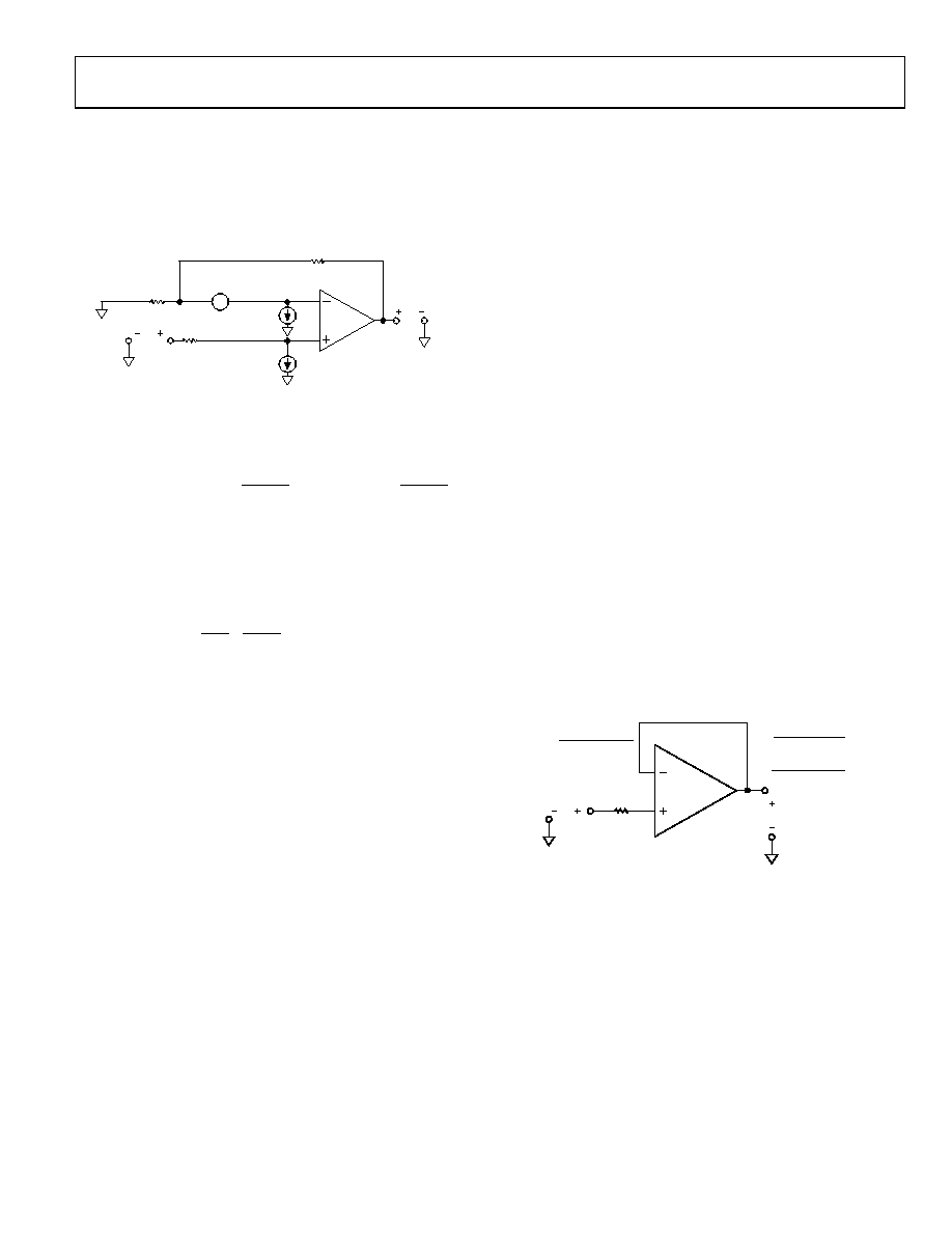
INPUT PROTECTION
The inputs of the AD8065/AD8066 are protected with back-to-
back diodes between the input terminals as well as ESD diodes
to either power supply. This results in an input stage with picoamps
of input current that can withstand up to 1500 V ESD events
(human body model) with no degradation.
Excessive power dissipation through the protection devices
destroys or degrades the performance of the amplifier. Differ-
ential voltages greater than 0.7 V result in an input current of
approximately (|V+ V| 0.7 V)/RI, where RI is the resistance in
series with the inputs.
For input voltages beyond the positive supply, the input current
is approximately (VI VCC 0.7)/RI. Beyond the negative supply,
the input current is about (VI VEE + 0.7)/RI. If the inputs of the
amplifier are to be subjected to sustained differential voltages
greater than 0.7 V, or to input voltages beyond the amplifier
power supply, input current should be limited to 30 mA by an
RI
VI
VO
AD8065
RI >
(| V+–V– | – 0.7V)
30mA
FOR LARGE | V+ –V– |
RI >
(VI –VEE – 0.7V)
30mA
RI >
(VI –VEE + 0.7V)
30mA
FOR VI BEYOND
SUPPLY VOLTAGES
02916-E
-055
Figure 55. Current-Limiting Resistor
相关PDF资料 |
PDF描述 |
|---|---|
| IXBOD1-40R | IC DIODE MODULE BOD 0.7A 4000V |
| EL8201IS-T7 | IC OP AMP 200MHZ R-R 8-SOIC |
| IXBOD1-38R | IC DIODE MODULE BOD 0.7A 3800V |
| IXBOD1-36R | IC DIODE MODULE BOD 0.7A 3600V |
| AD8034ARTZ-REEL | IC OPAMP VF R-R DUAL LN SOT23-8 |
相关代理商/技术参数 |
参数描述 |
|---|---|
| AD8065ARTZ-REEL7 | 功能描述:IC OPAMP VF R-R LN LP SOT23-5 RoHS:是 类别:集成电路 (IC) >> Linear - Amplifiers - Instrumentation 系列:FastFET™ 产品培训模块:Differential Circuit Design Techniques for Communication Applications 标准包装:1 系列:- 放大器类型:RF/IF 差分 电路数:1 输出类型:差分 转换速率:9800 V/µs 增益带宽积:- -3db带宽:2.9GHz 电流 - 输入偏压:3µA 电压 - 输入偏移:- 电流 - 电源:40mA 电流 - 输出 / 通道:- 电压 - 电源,单路/双路(±):3 V ~ 3.6 V 工作温度:-40°C ~ 85°C 安装类型:表面贴装 封装/外壳:16-VQFN 裸露焊盘,CSP 供应商设备封装:16-LFCSP-VQ 包装:剪切带 (CT) 产品目录页面:551 (CN2011-ZH PDF) 其它名称:ADL5561ACPZ-R7CT |
| AD8065ARTZ-REEL7 | 制造商:Analog Devices 功能描述:IC, OP-AMP, 145MHZ, 180V/ us, SOT-23-5 |
| AD8065ARZ | 功能描述:IC OPAMP VF R-R LN LP 30MA 8SOIC RoHS:是 类别:集成电路 (IC) >> Linear - Amplifiers - Instrumentation 系列:FastFET™ 产品培训模块:Differential Circuit Design Techniques for Communication Applications 标准包装:1 系列:- 放大器类型:RF/IF 差分 电路数:1 输出类型:差分 转换速率:9800 V/µs 增益带宽积:- -3db带宽:2.9GHz 电流 - 输入偏压:3µA 电压 - 输入偏移:- 电流 - 电源:40mA 电流 - 输出 / 通道:- 电压 - 电源,单路/双路(±):3 V ~ 3.6 V 工作温度:-40°C ~ 85°C 安装类型:表面贴装 封装/外壳:16-VQFN 裸露焊盘,CSP 供应商设备封装:16-LFCSP-VQ 包装:剪切带 (CT) 产品目录页面:551 (CN2011-ZH PDF) 其它名称:ADL5561ACPZ-R7CT |
| AD8065ARZ | 制造商:Analog Devices 功能描述:Operational Amplifier (Op-Amp) IC |
| AD8065ARZ-REEL | 功能描述:IC OPAMP VF R-R LN LP 30MA 8SOIC RoHS:是 类别:集成电路 (IC) >> Linear - Amplifiers - Instrumentation 系列:FastFET™ 标准包装:50 系列:- 放大器类型:通用 电路数:2 输出类型:满摆幅 转换速率:1.8 V/µs 增益带宽积:6.5MHz -3db带宽:4.5MHz 电流 - 输入偏压:5nA 电压 - 输入偏移:100µV 电流 - 电源:65µA 电流 - 输出 / 通道:35mA 电压 - 电源,单路/双路(±):1.8 V ~ 5.25 V,±0.9 V ~ 2.625 V 工作温度:-40°C ~ 85°C 安装类型:表面贴装 封装/外壳:10-TFSOP,10-MSOP(0.118",3.00mm 宽) 供应商设备封装:10-MSOP 包装:管件 |
发布紧急采购,3分钟左右您将得到回复。