- 您现在的位置:买卖IC网 > PDF目录16932 > AD8066ARM-EBZ (Analog Devices Inc)BOARD EVAL FOR AD8066ARM PDF资料下载
参数资料
| 型号: | AD8066ARM-EBZ |
| 厂商: | Analog Devices Inc |
| 文件页数: | 14/29页 |
| 文件大小: | 0K |
| 描述: | BOARD EVAL FOR AD8066ARM |
| 标准包装: | 1 |
| 每 IC 通道数: | 2 - 双 |
| 放大器类型: | 电压反馈 |
| 板类型: | 裸(未填充) |
| 已供物品: | 板 |
| 已用 IC / 零件: | 8-MSOP 封装 |
第1页第2页第3页第4页第5页第6页第7页第8页第9页第10页第11页第12页第13页当前第14页第15页第16页第17页第18页第19页第20页第21页第22页第23页第24页第25页第26页第27页第28页第29页
AD8065/AD8066
Rev. J | Page 20 of 28
THEORY OF OPERATION
The AD8065/AD8066 are voltage feedback operational amplifiers
that combine a laser-trimmed JFET input stage with the Analog
Devices eXtra Fast Complementary Bipolar (XFCB) process,
resulting in an outstanding combination of precision and speed.
The supply voltage range is from 5 V to 24 V. The amplifiers feature
a patented rail-to-rail output stage capable of driving within 0.5 V
of either power supply while sourcing or sinking up to 30 mA.
Also featured is a single-supply input stage that handles common-
mode signals from below the negative supply to within 3 V of the
positive rail. Operation beyond the JFET input range is possible
because of an auxiliary bipolar input stage that functions with
input voltages up to the positive supply. The amplifiers operate as
if they have a rail-to-rail input and exhibit no phase reversal
behavior for common-mode voltages within the power supply.
With voltage noise of 7 nV/√Hz and 88 dBc distortion for
1 MHz, 2 V p-p signals, the AD8065/AD8066 are a great choice
for high resolution data acquisition systems. Their low noise,
sub-pA input current, precision offset, and high speed make
them superb preamps for fast photodiode applications. The
speed and output drive capability of the AD8065/AD8066 also
make them useful in video applications.
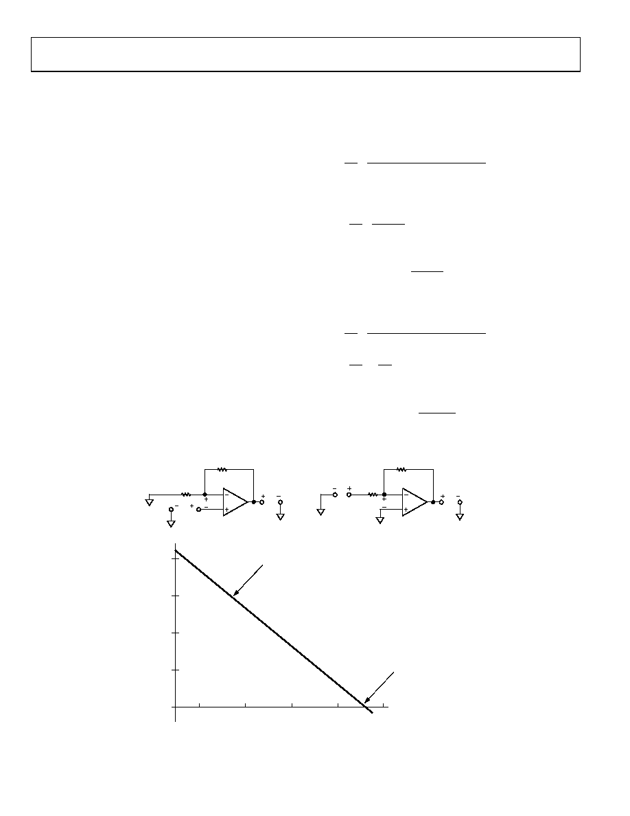
CLOSED-LOOP FREQUENCY RESPONSE
The AD8065/AD8066 are classic voltage feedback amplifiers
with an open-loop frequency response that can be approximated as
the integrator response shown in Figure 53. Basic closed-loop
frequency response for inverting and noninverting configurations
can be derived from the schematics shown.
NONINVERTING CLOSED-LOOP FREQUENCY
RESPONSE
Solving for the transfer function
()
G
crossover
G
F
G
crossover
I
O
R
f
s
R
f
V
×
π
+
×
π
=
2
where fcrossover is the frequency where the amplifier’s open-loop
gain equals 0 db
At dc
G
F
I
O
R
V
+
=
Closed-loop 3 dB frequency
G
F
G
crossover
3dB
R
f
+
×
=
INVERTING CLOSED-LOOP FREQUENCY
RESPONSE
()
G
crossover
G
F
crossover
I
O
R
f
R
s
R
f
V
×
π
+
×
π
=
2
At dc
G
F
I
O
R
V
=
Closed-loop 3 dB frequency
G
F
G
crossover
dB
R
f
+
×
=
3
RF
A
VO
RG
VI
VE
FREQUENCY (MHz)
80
60
0.01
100
OP
E
N
-LOOP
GAI
N
(A)
(dB)
0.1
10
1
40
20
0
fcrossover = 65MHz
A = (2
π× fcrossover)/s
RF
VE
A
VO
RG
VI
02916-E
-053
Figure 53. Open-Loop Gain vs. Frequency and Basic Connections
相关PDF资料 |
PDF描述 |
|---|---|
| 2-556212-3 | CABLE ASSY PWR-PWR 5 WIRE 180" |
| RCC18DCAH-S189 | CONN EDGECARD 36POS R/A .100 SLD |
| 381LX223M025K452 | CAP ALUM 22000UF 25V 20% SNAP |
| USB-5PSMBUS-CABLEZ | CABLE SMBUS USB 5PIN |
| AD8397AR-EBZ | BOARD EVAL FOR AD8397AR |
相关代理商/技术参数 |
参数描述 |
|---|---|
| AD8066ARM-REEL | 制造商:Analog Devices 功能描述:OP Amp Dual Volt Fdbk R-R O/P ±12V/24V 8-Pin MSOP T/R |
| AD8066ARM-REEL7 | 制造商:Analog Devices 功能描述:OP Amp Dual Volt Fdbk R-R O/P ±12V/24V 8-Pin MSOP T/R |
| AD8066ARMZ | 功能描述:IC OPAMP VF R-R DUAL LN LP 8MSOP RoHS:是 类别:集成电路 (IC) >> Linear - Amplifiers - Instrumentation 系列:FastFET™ 标准包装:2,500 系列:- 放大器类型:通用 电路数:4 输出类型:- 转换速率:0.6 V/µs 增益带宽积:1MHz -3db带宽:- 电流 - 输入偏压:45nA 电压 - 输入偏移:2000µV 电流 - 电源:1.4mA 电流 - 输出 / 通道:40mA 电压 - 电源,单路/双路(±):3 V ~ 32 V,±1.5 V ~ 16 V 工作温度:0°C ~ 70°C 安装类型:表面贴装 封装/外壳:14-TSSOP(0.173",4.40mm 宽) 供应商设备封装:14-TSSOP 包装:带卷 (TR) 其它名称:LM324ADTBR2G-NDLM324ADTBR2GOSTR |
| AD8066ARMZ | 制造商:Analog Devices 功能描述:Operational Amplifier (Op-Amp) IC |
| AD8066ARMZ-REEL7 | 功能描述:IC OPAMP VF R-R DUAL LN LP 8MSOP RoHS:是 类别:集成电路 (IC) >> Linear - Amplifiers - Instrumentation 系列:FastFET™ 标准包装:100 系列:- 放大器类型:通用 电路数:1 输出类型:- 转换速率:0.2 V/µs 增益带宽积:- -3db带宽:- 电流 - 输入偏压:100pA 电压 - 输入偏移:30µV 电流 - 电源:380µA 电流 - 输出 / 通道:- 电压 - 电源,单路/双路(±):±2 V ~ 18 V 工作温度:0°C ~ 70°C 安装类型:表面贴装 封装/外壳:8-SOIC(0.154",3.90mm 宽) 供应商设备封装:8-SO 包装:管件 |
发布紧急采购,3分钟左右您将得到回复。