参数资料
| 型号: | AD8099ARDZ |
| 厂商: | Analog Devices Inc |
| 文件页数: | 9/29页 |
| 文件大小: | 0K |
| 描述: | IC OPAMP VF ULN ULDIST 8SOIC |
| 产品培训模块: | Practical Guide High Speed PCB Layout |
| 标准包装: | 98 |
| 放大器类型: | 电压反馈 |
| 电路数: | 1 |
| 转换速率: | 1350 V/µs |
| -3db带宽: | 510MHz |
| 电流 - 输入偏压: | 6µA |
| 电压 - 输入偏移: | 100µV |
| 电流 - 电源: | 15mA |
| 电流 - 输出 / 通道: | 178mA |
| 电压 - 电源,单路/双路(±): | 5 V ~ 12 V,±2.5 V ~ 6 V |
| 工作温度: | -40°C ~ 125°C |
| 安装类型: | 表面贴装 |
| 封装/外壳: | 8-SOIC(0.154",3.90mm Width)裸露焊盘 |
| 供应商设备封装: | 8-SOIC-EP |
| 包装: | 管件 |
| 产品目录页面: | 770 (CN2011-ZH PDF) |
第1页第2页第3页第4页第5页第6页第7页第8页当前第9页第10页第11页第12页第13页第14页第15页第16页第17页第18页第19页第20页第21页第22页第23页第24页第25页第26页第27页第28页第29页
AD8099
Data Sheet
Rev. D | Page 16 of 28
APPLICATIONS
USING THE AD8099
The AD8099 offers unrivaled noise and distortion performance
in low signal gain configurations. In low gain configurations
(less than15), the AD8099 requires external compensation. The
amount of gain and performance needed will determine the
compensation network.
Understanding the subtleties of the AD8099 gives the user
insight on how to exact its peak performance. Use the
component values and circuit configurations shown in the
Applications section as starting points for designs. Specific
circuit applications will dictate the final configuration and value
of your components.
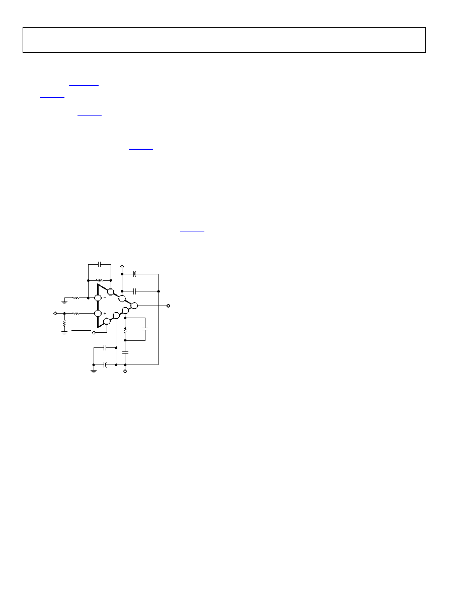
CIRCUIT COMPONENTS
The circuit components are referenced in Figure 59, the
recommended noninverting circuit schematic for the AD8099.
See Table 4 for typical component values and performance data.
1
8
4
7
5
3
6
2
AD8099
C5
0.1
F
CC
CF
C1
C4
10
F
C2
10
F
C3
0.1
F
RC
RF
RG
RS
R1
+VS
–VS
VOUT
DISABLE
04511-0-061
VIN
Figure 59. Wideband Noninverting Gain Configuration (SOIC)
RF and RG
—The feedback resistor and the gain set resistor
determine the noise gain of the amplifier; typical RF values
range from 250 to 499 .
CF
—Creates a zero in the loop response to compensate the pole
created by the input capacitance (including stray capacitance)
and the feedback resistor RF. CF helps reduce high frequency
peaking and ringing in the closed-loop response. Typical range
is 0.5 pF to 1.5 pF for evaluation circuits used here.
R1
—This resistor terminates the input of the amplifier to the
source resistance of the signal source, typically 50 . (This is
application specific and not always required.)
RS
—Many high speed amplifiers in low gain configurations
require that the input stage be terminated into a nominal
impedance to maintain stability. The value of RS should be kept
to 50 or lower to maintain low noise performance. At higher
gains, RS may be reduced or even eliminated. Typical range is
0 to 50 .
CC
—The compensation capacitor decreases the open-loop gain
at higher frequencies where the phase is degrading. By decreas-
ing the open-loop gain here, the phase margin is increased and
the amplifier is stabilized. Typical range is 0 pF to 5 pF. The
value of CC is gain dependent.
RC—
The series lead inductance of the package and the com-
pensation capacitance (CC) forms a series resonant circuit. RC
dampens this resonance and prevents oscillations. The
recommended value of RC is 50 for a closed-loop gain of 2.
This resistor introduces a zero in the open-loop response and
must be kept low so that this zero occurs at a higher frequency.
The purpose of the compensation network is to decrease the
open-loop gain. If the resistance becomes too large, the gain will
be reduced to the resistor value, and not necessarily to 0 ,
which is what a single capacitor would do over frequency.
Typical value range is 0 to 50 .
C1
—To lower the impedance of RC , C1 is placed in parallel with
RC. C1 is not required, but greatly reduces peaking at low
closed-loop gains. The typical value range is 0 pF to 2 pF.
C2 and C3
—Bypass capacitors are connected between both
supplies for optimum distortion and PSRR performance. These
capacitors should be placed as close as possible to the supply
pins of the amplifier. For C3, C5, a 0508 case size should be
used. The 0508 case size offers reduced inductance and better
frequency response.
C4 and C2
—Electrolytic bypass capacitors.
相关PDF资料 |
PDF描述 |
|---|---|
| AD8099ARD | IC OPAMP VF ULN ULDIST 8SOIC |
| OP482GSZ | IC OPAMP JFET 4MHZ QUAD 14SOIC |
| 2036-60-A | GAS DISCHARGE TUBE MINI 3 POLE |
| 2036-20-A | GAS DISCHARGE TUBE MINI 3 POLE |
| 2026-42-A | GAS DISCHARGE TUBE 3 POLE |
相关代理商/技术参数 |
参数描述 |
|---|---|
| AD8099ARDZ-REEL | 功能描述:IC OPAMP VF ULN ULDIST 8SOIC RoHS:是 类别:集成电路 (IC) >> Linear - Amplifiers - Instrumentation 系列:- 标准包装:50 系列:LinCMOS™ 放大器类型:通用 电路数:4 输出类型:- 转换速率:0.05 V/µs 增益带宽积:110kHz -3db带宽:- 电流 - 输入偏压:0.7pA 电压 - 输入偏移:210µV 电流 - 电源:57µA 电流 - 输出 / 通道:30mA 电压 - 电源,单路/双路(±):3 V ~ 16 V,±1.5 V ~ 8 V 工作温度:-40°C ~ 85°C 安装类型:表面贴装 封装/外壳:14-SOIC(0.154",3.90mm 宽) 供应商设备封装:14-SOIC 包装:管件 产品目录页面:865 (CN2011-ZH PDF) 其它名称:296-1834296-1834-5 |
| AD8099ARDZ-REEL7 | 功能描述:IC OPAMP VF ULN ULDIST 8SOIC RoHS:是 类别:集成电路 (IC) >> Linear - Amplifiers - Instrumentation 系列:- 标准包装:50 系列:LinCMOS™ 放大器类型:通用 电路数:4 输出类型:- 转换速率:0.05 V/µs 增益带宽积:110kHz -3db带宽:- 电流 - 输入偏压:0.7pA 电压 - 输入偏移:210µV 电流 - 电源:57µA 电流 - 输出 / 通道:30mA 电压 - 电源,单路/双路(±):3 V ~ 16 V,±1.5 V ~ 8 V 工作温度:-40°C ~ 85°C 安装类型:表面贴装 封装/外壳:14-SOIC(0.154",3.90mm 宽) 供应商设备封装:14-SOIC 包装:管件 产品目录页面:865 (CN2011-ZH PDF) 其它名称:296-1834296-1834-5 |
| AD8099CP-R2 | 制造商:Analog Devices 功能描述:OP AMP SGL VOLT FDBK 6V/12V 8LFCSP - Tape and Reel |
| AD809BR | 制造商:Rochester Electronics LLC 功能描述:155.52MHZ FREQUENCY SYNTH - Bulk 制造商:Analog Devices 功能描述:Frequency Synthesizer, 16 Pin, Plastic, SOP |
| AD809BR-REEL7 | 功能描述:IC SYNTH FREQ 155.52MHZ 16-SOIC RoHS:否 类别:集成电路 (IC) >> 时钟/计时 - 时钟发生器,PLL,频率合成器 系列:- 标准包装:1,000 系列:Precision Edge® 类型:时钟/频率合成器 PLL:无 输入:CML,PECL 输出:CML 电路数:1 比率 - 输入:输出:2:1 差分 - 输入:输出:是/是 频率 - 最大:10.7GHz 除法器/乘法器:无/无 电源电压:2.375 V ~ 3.6 V 工作温度:-40°C ~ 85°C 安装类型:表面贴装 封装/外壳:16-VFQFN 裸露焊盘,16-MLF? 供应商设备封装:16-MLF?(3x3) 包装:带卷 (TR) 其它名称:SY58052UMGTRSY58052UMGTR-ND |
发布紧急采购,3分钟左右您将得到回复。