- 您现在的位置:买卖IC网 > PDF目录10791 > AD8123ACPZ-R7 (Analog Devices Inc)IC RCVR TRPL DIFF EQUAL 40LFCSP PDF资料下载
参数资料
| 型号: | AD8123ACPZ-R7 |
| 厂商: | Analog Devices Inc |
| 文件页数: | 7/16页 |
| 文件大小: | 0K |
| 描述: | IC RCVR TRPL DIFF EQUAL 40LFCSP |
| 标准包装: | 1 |
| 类型: | 接收器 |
| 驱动器/接收器数: | 0/3 |
| 电源电压: | 4.5 V ~ 5.5 V |
| 安装类型: | 表面贴装 |
| 封装/外壳: | 40-VFQFN 裸露焊盘,CSP |
| 供应商设备封装: | 40-LFCSP-VQ(6x6) |
| 包装: | 标准包装 |
| 产品目录页面: | 765 (CN2011-ZH PDF) |
| 其它名称: | AD8123ACPZ-R7DKR |
AD8123
Rev. A | Page 15 of 16
INPUT COMMON-MODE RANGE
When used, common-mode sync signals are generally applied
with a peak deviation of 500 mV and thereby increase the
common-mode level from 2.675 V to 3.175 V. This common-
mode level exceeds the specified input voltage swing limits of
±3.0 V; therefore, the AD8123 cannot be used with a system
that uses common-mode sync encoding with 500 mV sync peak
deviation and 2.5 V common-mode line level. While it is possible
to operate a driver powered from a single 5 V supply at a common-
mode voltage of <2.5 V to obtain a received voltage swing that is
within the specified limits, there is not much margin for other
shifts in the common-mode level due to interference pickup and
differing ground potentials. There are two ways to increase the
common-mode range of the overall system. One is to power the
driver from ±5 V supplies, and the other is to place an AD8143
in front of the AD8123, as shown in Figure 32. These techniques
may be combined or applied separately.
Most applications that use the AD8123 as a receiver use a driver
(such as one from the AD8146/AD8147/AD8148 family, the
places the common-mode voltage on the line nominally at 0 V
relative to the ground potential at the driver and provides optimum
immunity from any common-mode anomalies picked up along
the cable (including ground shifts between the driver and receiver
ends). In many of these applications, the AD8123 input voltage
range of typically ±3.0 V is sufficient. If wider input range is
required, the AD8143 triple receiver (input common-mode
range equals ±10.5 V on ±12 V supplies) may be placed in front of
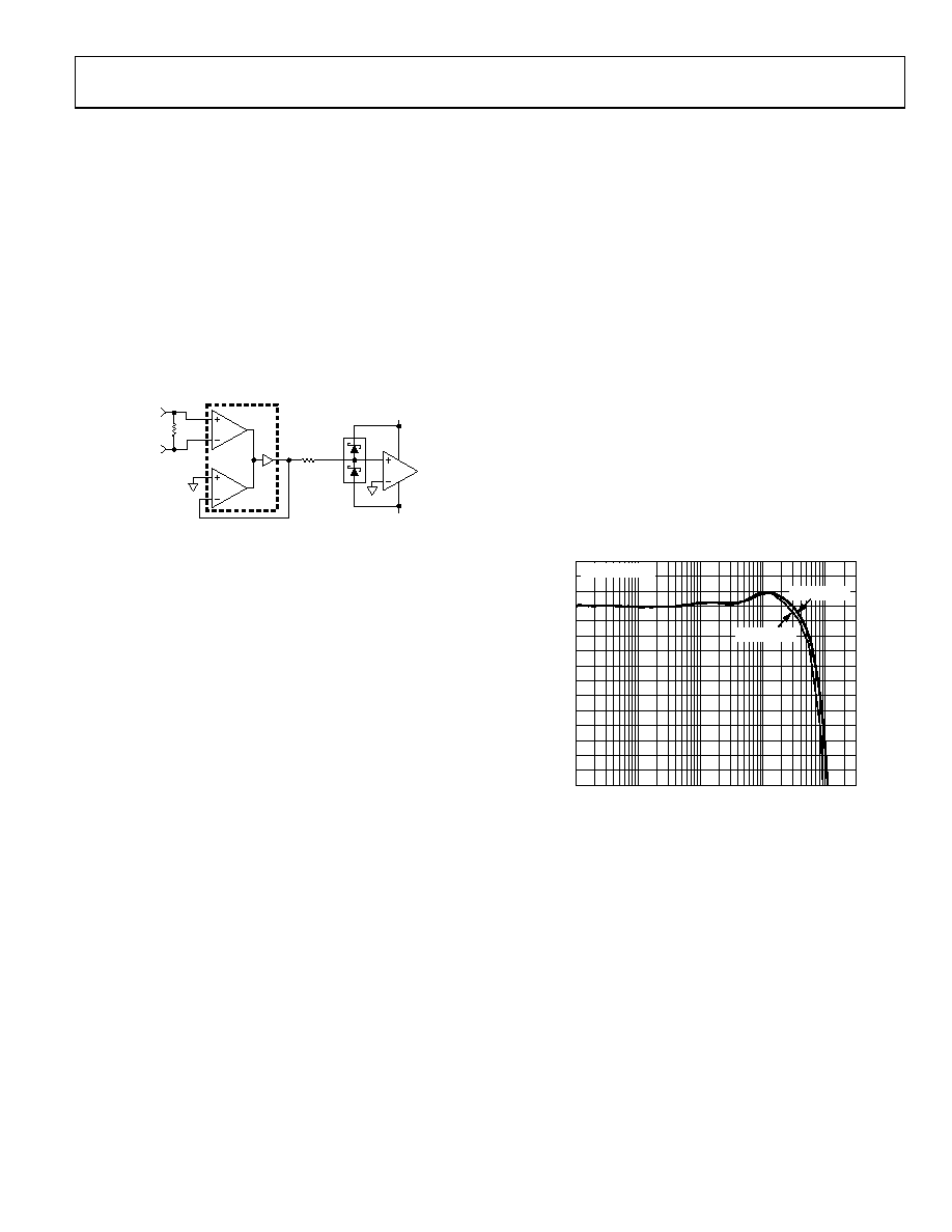
the AD8123. Figure 32 illustrates how this is done for one channel.
068
14-
03
3
100
49.9
1
2
3
RECEIVED
SIGNAL
+5V
ONE AD8123
INPUT
ONE AD8143 CHANNE L
POWER SUPPLIES = ±12V
–5V
HBAT-540C
SMALL SIGNAL FREQUENCY RESPONSE
Though the AD8123 large signal frequency response
(VO = 1 V p-p) is of most concern, occasionally designers are
interested in the small signal frequency response. The AD8123
for 200 meter and 300 meter cable lengths.
Figure 32. Optional Use of AD8143 in Front of AD8123 for
Wide Input Common-Mode Range
06
81
4-
0
32
FREQUENCY (MHz)
GA
IN
(
d
B
)
–12
–11
–10
–9
–8
–7
–6
–5
–4
–3
–2
–1
0
1
2
3
0.1
1
10
100
0.01
VO = 300mV p-p
200 METERS
300 METERS
The Schottky diodes are required to protect the AD8123 from
any AD8143 outputs that may exceed the AD8123 input limits.
The 49.9 Ω resistor limits the fault current and produces a pole
at approximately 800 MHz with the effective diode capacitance of
3 pF and the AD8123 input capacitance of 1 pF. The pole drops
the response by only 0.07 dB at 100 MHz and therefore has a
negligible effect on the signal.
When using a single 5 V supply on the driver side, the common-
mode voltage at the driver is typically midsupply, or VCM = 2.5 V.
The largest received differential video signal is approximately
700 mV p-p, and this therefore adds 175 mVPEAK to the common-
mode voltage, resulting in a worst-case peak voltage of 2.675 V
on an AD8123 input (presuming there is no ground shift between
driver and receiver). This is within the AD8123 input voltage
swing limits, and such a system works well as long as the difference
in ground potential between driver and receiver does not cause
the input voltage swing to exceed its specified limits.
Figure 33. Small Signal Frequency Response for Various Cable Lengths
POWER-DOWN
The power-down feature is intended to be used to reduce power
consumption when a particular device is not in use and does
not place the output in a high-Z state when asserted. The input
logic levels and supply current in power-down mode are presented
in the Power Supply section of Table 1.
相关PDF资料 |
PDF描述 |
|---|---|
| AD5384BBC-3 | IC DAC 14BIT 40CH 3V 100-CSPBGA |
| AD5384BBC-3REEL7 | IC DAC 14BIT 40CH 3V 100-CSPBGA |
| ADCMP572BCPZ-R2 | IC COMPARATOR CML 3.3-5V 16LFCSP |
| LTC1687IS#PBF | IC TXRX RS485 PREC DELAY 14-SOIC |
| LTC1686IS8#PBF | IC TXRX RS485 PREC DELAY 8-SOIC |
相关代理商/技术参数 |
参数描述 |
|---|---|
| AD8123ACPZ-R71 | 制造商:AD 制造商全称:Analog Devices 功能描述:Triple Differential Receiver with Adjustable Line Equalization |
| AD8123ACPZ-RL | 功能描述:IC RCVR TRPL DIFF EQUAL 40LFCSP RoHS:是 类别:集成电路 (IC) >> 接口 - 驱动器,接收器,收发器 系列:- 标准包装:250 系列:- 类型:收发器 驱动器/接收器数:2/2 规程:RS232 电源电压:3 V ~ 5.5 V 安装类型:表面贴装 封装/外壳:16-TSSOP(0.173",4.40mm 宽) 供应商设备封装:16-TSSOP 包装:带卷 (TR) |
| AD8123ACPZ-RL1 | 制造商:AD 制造商全称:Analog Devices 功能描述:Triple Differential Receiver with Adjustable Line Equalization |
| AD8123ACPZ-TR | 制造商:Analog Devices 功能描述:TRIPLE EQUALIZER - Tape and Reel |
| AD8124 | 制造商:AD 制造商全称:Analog Devices 功能描述:Triple Differential Receiver with 200 Meter Adjustable Cable Equalization |
发布紧急采购,3分钟左右您将得到回复。