参数资料
| 型号: | AD8150ASTZ |
| 厂商: | Analog Devices Inc |
| 文件页数: | 20/44页 |
| 文件大小: | 0K |
| 描述: | IC CROSSPOINT SWIT 33X17 184LQFP |
| 标准包装: | 1 |
| 系列: | XStream™ |
| 功能: | 交叉点开关 |
| 电路: | 1 x 33:17 |
| 电压电源: | 双电源 |
| 电压 - 电源,单路/双路(±): | ±3 V ~ 5.25 V |
| 工作温度: | 0°C ~ 85°C |
| 安装类型: | 表面贴装 |
| 封装/外壳: | 184-LQFP |
| 供应商设备封装: | 184-LQFP(20x20) |
| 包装: | 管件 |
第1页第2页第3页第4页第5页第6页第7页第8页第9页第10页第11页第12页第13页第14页第15页第16页第17页第18页第19页当前第20页第21页第22页第23页第24页第25页第26页第27页第28页第29页第30页第31页第32页第33页第34页第35页第36页第37页第38页第39页第40页第41页第42页第43页第44页
AD8150
Rev. A | Page 27 of 44
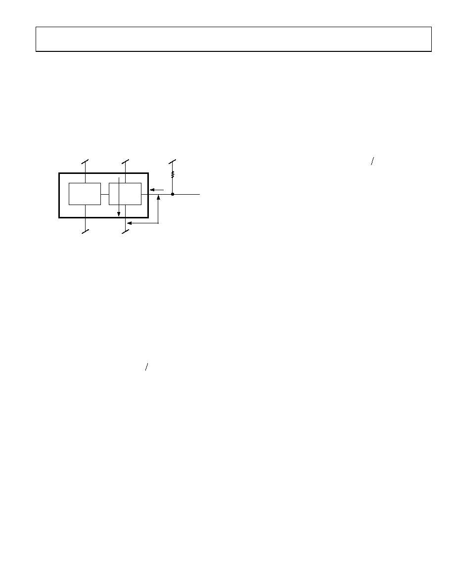
POWER DISSIPATION
For analysis, the power dissipation of the AD8150 can be
divided into three separate parts. These are the control logic,
the data path circuits, and the (ECL or PECL) outputs, which
are part of the data path circuits, but can be dealt with
separately. The first of these, the control logic, is CMOS
technology and does not dissipate a significant amount of
power. This power will, of course, be greater when the logic
supply is 5 V than when it is 3 V, but overall it is not a significant
amount of power and can be ignored for thermal analysis.
01074-040
DATA
PATHS
CONTROL
LOGIC
VCC
VDD
VEE
IOUT
ROUT
VOUT LOW – VEE
VSS
GND
AD8150
I, DATA PATH
LOGIC
Figure 41. Major Power Consumption Paths
The data path circuits operate between the supplies VCC and
VEE. As described in the power supply section, this voltage can
range from 3.3 V to 5 V. The current consumed by this section
will be constant, so operating at a lower voltage can save about
40 percent in power dissipation.
The power dissipated in the data path outputs is affected by
several factors. The first is whether the outputs are enabled or
disabled. The worst case occurs when all of the outputs are
enabled. The current consumed by the data path logic can be
approximated by
()
[
]
()
enabled
outputs
of
I
OUT
CC
#
mA
3
mA
20
mA
5
.
4
mA
30
×
+
=
This says that there will always be a minimum of 30 mA
flowing. ICC will increase by a factor that is proportional to both
the number of enabled outputs and the programmed output
current.
The power dissipated in this circuit section will simply be the
voltage of this section (VCC VEE) times the current. For a worst
case, assume that VCC VEE is 5.0 V, all outputs are enabled and
the programmed output current is 25 mA. The power dissipated
by the data path logic will be
()
[]
{
}
mW
826
17
mA
3
mA
20
mA
25
mA
5
.
4
mA
25
V
0
.
5
=
×
+
=
P
The power dissipated by the output current depends on several
factors. These are the programmed output current, the voltage
drop from a logic low output to VEE, and the number of enabled
outputs. A simplifying assumption is that one of each (enabled)
differential output pair will be low and draw the full output
current (and dissipate most of the power for that output), while
the complementary output of the pair will be high and draw
insignificant current. Thus, the power dissipation of the high
output can be ignored, and the output power dissipation for
each output can be assumed to occur in a single static low
output that sinks the full output-programmed current.
The voltage across which this current flows can also vary,
depending on the output circuit design and the supplies that are
used for the data path circuitry. In general, however, there will
be a voltage difference between a logic low signal and VEE. This
is the drop across which the output current flows. For a worst
case, this voltage can be as high as 3.5 V. Thus, for all outputs
enabled and the programmed output current set to 25 mA, the
power dissipated by the outputs is
(
)
W
49
.
1
17
mA
25
V
5
.
3
=
×
=
P
相关PDF资料 |
PDF描述 |
|---|---|
| AD8151ASTZ | IC CROSSPOINT SWIT 33X17 184LQFP |
| AD8152JBP | IC CROSSPOINT SWIT 34X34 256BGA |
| AD8153ACPZ-RL7 | IC SW MUX/DEMUX SGL BUFF 32LFCSP |
| AD8155ACPZ | IC MUX/DEMUX DUAL BUFFER 64LFCSP |
| AD8156ABCZ | IC SWITCH XPT 4X4 W/EQ 49CSPBGA |
相关代理商/技术参数 |
参数描述 |
|---|---|
| AD8150ASTZ | 制造商:Analog Devices 功能描述:IC DIGITAL CROSSPOINT SWITCH |
| AD8150-EVAL | 制造商:Analog Devices 功能描述:EVAL KIT FOR 33 17, 1.5 GBPS DGTL CROSSPOINT SWIT - Bulk |
| AD8151 | 制造商:AD 制造商全称:Analog Devices 功能描述:33 x 17, 3.2 Gb/s Digital Crosspoint Switch |
| AD8151AST | 制造商:AD 制造商全称:Analog Devices 功能描述:33 x 17, 3.2 Gb/s Digital Crosspoint Switch |
| AD8151ASTZ | 功能描述:IC CROSSPOINT SWIT 33X17 184LQFP RoHS:是 类别:集成电路 (IC) >> 接口 - 模拟开关,多路复用器,多路分解器 系列:XStream™ 其它有关文件:STG4159 View All Specifications 标准包装:5,000 系列:- 功能:开关 电路:1 x SPDT 导通状态电阻:300 毫欧 电压电源:双电源 电压 - 电源,单路/双路(±):±1.65 V ~ 4.8 V 电流 - 电源:50nA 工作温度:-40°C ~ 85°C 安装类型:表面贴装 封装/外壳:7-WFBGA,FCBGA 供应商设备封装:7-覆晶 包装:带卷 (TR) |
发布紧急采购,3分钟左右您将得到回复。