- 您现在的位置:买卖IC网 > PDF目录378276 > AD8152-EVAL (Analog Devices, Inc.) 34 x 34, 3.2 Gbps Asynchronous Digital Crosspoint Switch PDF资料下载
参数资料
| 型号: | AD8152-EVAL |
| 厂商: | Analog Devices, Inc. |
| 英文描述: | 34 x 34, 3.2 Gbps Asynchronous Digital Crosspoint Switch |
| 中文描述: | 34 × 34,3.2 Gbps的异步数字交叉点开关 |
| 文件页数: | 18/32页 |
| 文件大小: | 1351K |
| 代理商: | AD8152-EVAL |
第1页第2页第3页第4页第5页第6页第7页第8页第9页第10页第11页第12页第13页第14页第15页第16页第17页当前第18页第19页第20页第21页第22页第23页第24页第25页第26页第27页第28页第29页第30页第31页第32页
REV. A
–18–
AD8152
Input Coupling
One way to simplify the input circuit and make it compatible with
a wide variety of driving devices is to use ac coupling. This has
the effect of isolating the dc common-mode levels of the driver
and the AD8152 input circuitry. For example, the XAUI inter-
connect specification for 10 Gbps Ethernet requires ac coupling
in order to ensure that there are no interactions of dc levels
between the transmitting and receiving devices.
AC coupling requires that the signal patterns have no long-term
dc component, which may occur in any random data stream.
Codes such as 8b/10b, called for in the XAUI specification, are
used in many data communications systems to ensure that the
data pattern is benign in an ac-coupled link. This is accomplished
by run-length limiting (RLL), which sets a maximum for the
number of 1s or 0s that can occur consecutively. In addition,
residual dc components are monitored and modified by keeping
track of the running disparity, excess of 1s versus 0s or vice versa.
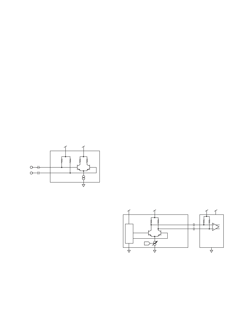
For the AD8152 inputs, ac coupling requires a capacitor in series
with each single-ended input signal, as shown in Figure 7. This
should be done in a manner that does not interfere with the high
speed signal integrity of the PC board. The details of this are
covered in the section on board layout guidelines. The two critical
variables are setting the proper voltage for VTTI and selecting
the correct value of coupling capacitors.
50
VTTI
VCC
50
VEE
INXXP
INXXN
C
INP
C
INN
Figure 7. AC-Coupling Input Signal from AD8152
On the AD8152 side of the input coupling capacitor, the average
value of the single-ended input voltage will be at the voltage set at
VTTI. The range of allowable voltages is a function of the accept-
able input voltages of the active circuitry of the AD8152 inputs
and the amplitude of the input signal. The operating input range
of the AD8152 extends from VCC + 0.2 V to 0.8 V above VEE.
The total range that will be occupied by the input signal will be
its average value (as established by the voltage applied to VTTI)
plus or minus one half the single-ended swing of the signal. For a
standard 800 mV p-p differential signal, the single-ended swing is
400 mV p-p. Thus, the signal will swing
±
200 mV about the
average value equal to VTTI.
If VTTI is set equal to VCC, then the single-ended signal will
just meet the specifications where its highest excursion will be
0.2 V higher than VCC. The lowest level to set VTTI is 0.8 V
above VEE. This will cause the negative signal excursions to stay
within the operating range.
With ac-coupled inputs, there is no power consumption advan-
tage associated with varying VTTI. As a practical matter, it
might be desirable to set VTTI at the same voltage as VTTO so
that only one supply is necessary. Refer to the VTTO section for
more information.
Output Coupling
Each single-ended output of the AD8152 has a termination
resistor that ties to a common point called VTTO. When VTTO
is varied, it will change the common-mode levels of the outputs
and the power dissipation of the output stages when they are
enabled.
The individual output currents are programmable. Varying this
current will change the lower level of the output voltage (and thus
the peak-to-peak swing) and also change the power dissipation in
the output stages. To obtain a standard 800 mV p-p differential
output (single-ended = 400 mV p-p), the output current should
be programmed to 16 mA. With an effective termination resis-
tance of 25
W
, this will generate the proper differential voltage.
If the AD8152 drives another device that is ac-coupled, there is no
interaction of the dc levels on each side of the coupling capacitors
(see Figure 8). The dc levels for the AD8152 can be calculated
independent of the levels of the device that is driven.
The upper allowable setting for VTTO is 0.2 V higher than VCC.
The signals will be pulled up to this level at their highest excursion.
However at this setting, the power dissipation will be a maximum.
To save power, VTTO can be lowered. The lowest level for
VTTO will be determined by the lowest output level allowable
(V
OL
) by the AD8152 output when it is logically low. The output
at any time should not go lower than 1.0 V below VCC. If the
single-ended swing of an output is 400 mV p-p, then the lowest
that VTTO can go is 0.6 V below VCC. For more information
on V
OL
, see TPC 17.
VTTO
VEE
I = 2mA (CODE) + 2mA
50
50
OUTXXP
OUTXXN
AD8152
VEE
VCC
VTT
VCC
DRIVEN DEVICE
VEE
Figure 8. AC-Coupling Output Signal from AD8152
相关PDF资料 |
PDF描述 |
|---|---|
| AD8152JBP | 34 x 34, 3.2 Gbps Asynchronous Digital Crosspoint Switch |
| AD82550A | Stereo Digital Audio Amplifier with Headphone Driver |
| AD82550A-CG | Stereo Digital Audio Amplifier with Headphone Driver |
| AD82551A | Stereo Digital Audio Amplifier with Headphone Driver |
| AD82551A-CG | Stereo Digital Audio Amplifier with Headphone Driver |
相关代理商/技术参数 |
参数描述 |
|---|---|
| AD8152JBP | 功能描述:IC CROSSPOINT SWIT 34X34 256BGA RoHS:否 类别:集成电路 (IC) >> 接口 - 模拟开关,多路复用器,多路分解器 系列:XStream™ 其它有关文件:STG4159 View All Specifications 标准包装:5,000 系列:- 功能:开关 电路:1 x SPDT 导通状态电阻:300 毫欧 电压电源:双电源 电压 - 电源,单路/双路(±):±1.65 V ~ 4.8 V 电流 - 电源:50nA 工作温度:-40°C ~ 85°C 安装类型:表面贴装 封装/外壳:7-WFBGA,FCBGA 供应商设备封装:7-覆晶 包装:带卷 (TR) |
| AD8152JBPZ | 功能描述:IC CROSSPOINT SWIT 34X34 256BGA RoHS:是 类别:集成电路 (IC) >> 接口 - 模拟开关,多路复用器,多路分解器 系列:XStream™ 应用说明:Ultrasound Imaging Systems Application Note 产品培训模块:Lead (SnPb) Finish for COTS Obsolescence Mitigation Program 标准包装:250 系列:- 功能:开关 电路:单刀单掷 导通状态电阻:48 欧姆 电压电源:单电源 电压 - 电源,单路/双路(±):2.7 V ~ 5.5 V 电流 - 电源:5µA 工作温度:0°C ~ 70°C 安装类型:表面贴装 封装/外壳:48-LQFP 供应商设备封装:48-LQFP(7x7) 包装:托盘 |
| AD8153 | 制造商:AD 制造商全称:Analog Devices 功能描述:3.2 Gbps Single Buffered Mux/Demux Switch |
| AD8153_07 | 制造商:AD 制造商全称:Analog Devices 功能描述:3.2 Gbps Single Buffered Mux/Demux Switch |
| AD8153ACPZ | 功能描述:IC SW MUX/DEMUX SGL BUFF 32LFCSP RoHS:是 类别:集成电路 (IC) >> 接口 - 专用 系列:XStream™ 特色产品:NXP - I2C Interface 标准包装:1 系列:- 应用:2 通道 I²C 多路复用器 接口:I²C,SM 总线 电源电压:2.3 V ~ 5.5 V 封装/外壳:16-TSSOP(0.173",4.40mm 宽) 供应商设备封装:16-TSSOP 包装:剪切带 (CT) 安装类型:表面贴装 产品目录页面:825 (CN2011-ZH PDF) 其它名称:568-1854-1 |
发布紧急采购,3分钟左右您将得到回复。