- 您现在的位置:买卖IC网 > PDF目录378276 > AD8152JBP (ANALOG DEVICES INC) 34 x 34, 3.2 Gbps Asynchronous Digital Crosspoint Switch PDF资料下载
参数资料
| 型号: | AD8152JBP |
| 厂商: | ANALOG DEVICES INC |
| 元件分类: | 运动控制电子 |
| 英文描述: | 34 x 34, 3.2 Gbps Asynchronous Digital Crosspoint Switch |
| 中文描述: | 34-CHANNEL, CROSS POINT SWITCH, PBGA256 |
| 封装: | 27 X 27 MM, 1.27 MM PITCH, PLASTIC, MO-192BAL-2, SBGA-256 |
| 文件页数: | 22/32页 |
| 文件大小: | 1351K |
| 代理商: | AD8152JBP |
第1页第2页第3页第4页第5页第6页第7页第8页第9页第10页第11页第12页第13页第14页第15页第16页第17页第18页第19页第20页第21页当前第22页第23页第24页第25页第26页第27页第28页第29页第30页第31页第32页
REV. A
–22–
AD8152
The variety of supply configurations cause the need for a supply
agile digital control circuitry. This is done by a programmable
logic device (PLD), which provides instructions to the AD8152.
The PLD supply is typically tied with jumpers across the AD8152’s
VCC and VEE supplies (Jumpers J3 and J4). The PLD is addressed
from the PC by way of digital isolators. These couplers isolate
PC levels from the PLD and allow for any level shifting. If
desired, the user can drive the PLD supply separately as long as
the VEE of the AD8152 and the PLD are tied together (remove
Jumper J3 and leave J4 installed). This allows one to measure
the AD8152 only supply current, for example.
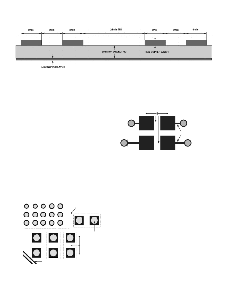
Board Construction or Stack-Up
Figure 11 is a picture of AD8152 evaluation board stack-up from
top to bottom. The layer stack-up has been made symmetrical
to avoid board warpage during manufacture. The microstrip
layout and dimensions are shown in Figure 12. The microstrip
trace width was chosen to be 8 mils. This allows relative ease in
routing through the BGA rows that are 50 mils (1.27 mm) apart.
The outer two out of four rows of high speed signals are routed on
top of the PCB, while the inner two rows are via holed to the
board’s opposite side and then routed outward. Wider microstrip
is desirable for reducing eye height loss versus long traces; how-
ever, the routing will be more difficult as the AD8152 is approached.
The wide microstrip would have to be necked down in width in
order to be routed into the BGA. The necking will increase trace
impedance and therefore induce more signal reflection problems.
MICROSTRIP TRACES
BGA CORNER OUTLINE
VIA HOLE
CHIP CAPACITOR
Figure 13. BGA Corner Capacitor Layout
Figure 12. Cross-Sectional Layout and Dimensioning (To Scale) of Differential
During the layout of the differential microstrip, a software tool
snaps the distance between the two traces to be a constant. If
the distance is not kept constant, impedance variations will
result. These fluctuations can be measured by time domain
reflectometry (TDR).
EXTRA ADDED INDUCTANCE
Figure 14. Poor Capacitor Layout
Bypass Capacitor Layout
The AD8152 8-layer PCB takes advantage of buried interlayer
capacitance. The VEE to VCC planes are placed in the very middle
of the board to make the highest value capacitor. The 4 mil
(0.102 mm) dielectric spacing between VCC/VEE yields 26 nF
of capacitance. Each AD8152 supply pin is directly connected to
its supply plane through a via hole beneath the BGA ball. The
via hole size for a BGA supply pin is slightly bigger than a signal
via. This is to reduce the inductance of the connection, and it
also happens to be a compact layout.
For the chip capacitors, the via holes are placed directly in the
middle of the mounting area and made as large as possible, i.e.,
greater than or equal to 35 mils (0.89 mm). This is to minimize
inductance as much as possible. By minimizing inductance, the
performance of the capacitor or impedance versus frequency
response is not greatly diminished. Note that chip capacitors
will work up to only about 300 MHz.
Figure 14 is an example of a bypass capacitor layout that should
be avoided in any high speed printed circuit board. This layout
connects the chip capacitor mounting pads to small via holes
through a skinny PCB trace. This amounts to four extra inductors
added to the capacitor, two largely from the skinny surface traces
and two from small via holes. Inductance is also variable with
copper thickness and attachment method to power plane. Thermal
relief for soldering purposes also adds unwanted inductance and
should be avoided.
相关PDF资料 |
PDF描述 |
|---|---|
| AD82550A | Stereo Digital Audio Amplifier with Headphone Driver |
| AD82550A-CG | Stereo Digital Audio Amplifier with Headphone Driver |
| AD82551A | Stereo Digital Audio Amplifier with Headphone Driver |
| AD82551A-CG | Stereo Digital Audio Amplifier with Headphone Driver |
| AD8256A | 2x16W Stereo Digital Audio Amplifier with Headphone Driver |
相关代理商/技术参数 |
参数描述 |
|---|---|
| AD8152JBPZ | 功能描述:IC CROSSPOINT SWIT 34X34 256BGA RoHS:是 类别:集成电路 (IC) >> 接口 - 模拟开关,多路复用器,多路分解器 系列:XStream™ 应用说明:Ultrasound Imaging Systems Application Note 产品培训模块:Lead (SnPb) Finish for COTS Obsolescence Mitigation Program 标准包装:250 系列:- 功能:开关 电路:单刀单掷 导通状态电阻:48 欧姆 电压电源:单电源 电压 - 电源,单路/双路(±):2.7 V ~ 5.5 V 电流 - 电源:5µA 工作温度:0°C ~ 70°C 安装类型:表面贴装 封装/外壳:48-LQFP 供应商设备封装:48-LQFP(7x7) 包装:托盘 |
| AD8153 | 制造商:AD 制造商全称:Analog Devices 功能描述:3.2 Gbps Single Buffered Mux/Demux Switch |
| AD8153_07 | 制造商:AD 制造商全称:Analog Devices 功能描述:3.2 Gbps Single Buffered Mux/Demux Switch |
| AD8153ACPZ | 功能描述:IC SW MUX/DEMUX SGL BUFF 32LFCSP RoHS:是 类别:集成电路 (IC) >> 接口 - 专用 系列:XStream™ 特色产品:NXP - I2C Interface 标准包装:1 系列:- 应用:2 通道 I²C 多路复用器 接口:I²C,SM 总线 电源电压:2.3 V ~ 5.5 V 封装/外壳:16-TSSOP(0.173",4.40mm 宽) 供应商设备封装:16-TSSOP 包装:剪切带 (CT) 安装类型:表面贴装 产品目录页面:825 (CN2011-ZH PDF) 其它名称:568-1854-1 |
| AD8153ACPZ-RL7 | 功能描述:IC SW MUX/DEMUX SGL BUFF 32LFCSP RoHS:是 类别:集成电路 (IC) >> 接口 - 专用 系列:XStream™ 特色产品:NXP - I2C Interface 标准包装:1 系列:- 应用:2 通道 I²C 多路复用器 接口:I²C,SM 总线 电源电压:2.3 V ~ 5.5 V 封装/外壳:16-TSSOP(0.173",4.40mm 宽) 供应商设备封装:16-TSSOP 包装:剪切带 (CT) 安装类型:表面贴装 产品目录页面:825 (CN2011-ZH PDF) 其它名称:568-1854-1 |
发布紧急采购,3分钟左右您将得到回复。