参数资料
| 型号: | AD8158ACPZ |
| 厂商: | Analog Devices Inc |
| 文件页数: | 8/36页 |
| 文件大小: | 0K |
| 描述: | IC MUX/DEMUX QUAD 2X1 100LFCSP |
| 产品变化通告: | AD8158 Change of Default Settings 13/Aug/2009 |
| 标准包装: | 1 |
| 系列: | XStream™ |
| 功能: | 多路复用器/多路分解器 |
| 电路: | 4 x 2:1 |
| 电压电源: | 单电源 |
| 电压 - 电源,单路/双路(±): | 1.6 V ~ 3.6 V |
| 电流 - 电源: | 780mA |
| 工作温度: | -40°C ~ 85°C |
| 安装类型: | 表面贴装 |
| 封装/外壳: | 100-VFQFN 裸露焊盘,CSP |
| 供应商设备封装: | 100ピンLFCSP-VQ(12x12) |
| 包装: | 托盘 |
第1页第2页第3页第4页第5页第6页第7页当前第8页第9页第10页第11页第12页第13页第14页第15页第16页第17页第18页第19页第20页第21页第22页第23页第24页第25页第26页第27页第28页第29页第30页第31页第32页第33页第34页第35页第36页
AD8158
Rev. B | Page 16 of 36
THEORY OF OPERATION
The AD8158 is a buffered, asynchronous, three-port transceiver
that allows 2:1 multiplexing and 1:2 demultiplexing among its
ports. The 1:2 demux path supports bicast operation, allowing
the AD8158 to operate as a port replicator as well as a redundancy
switch. The AD8158 offers loopback on each lane, allowing
the part to be configured as a twelve-lane equalizer or redriver
with FFE.
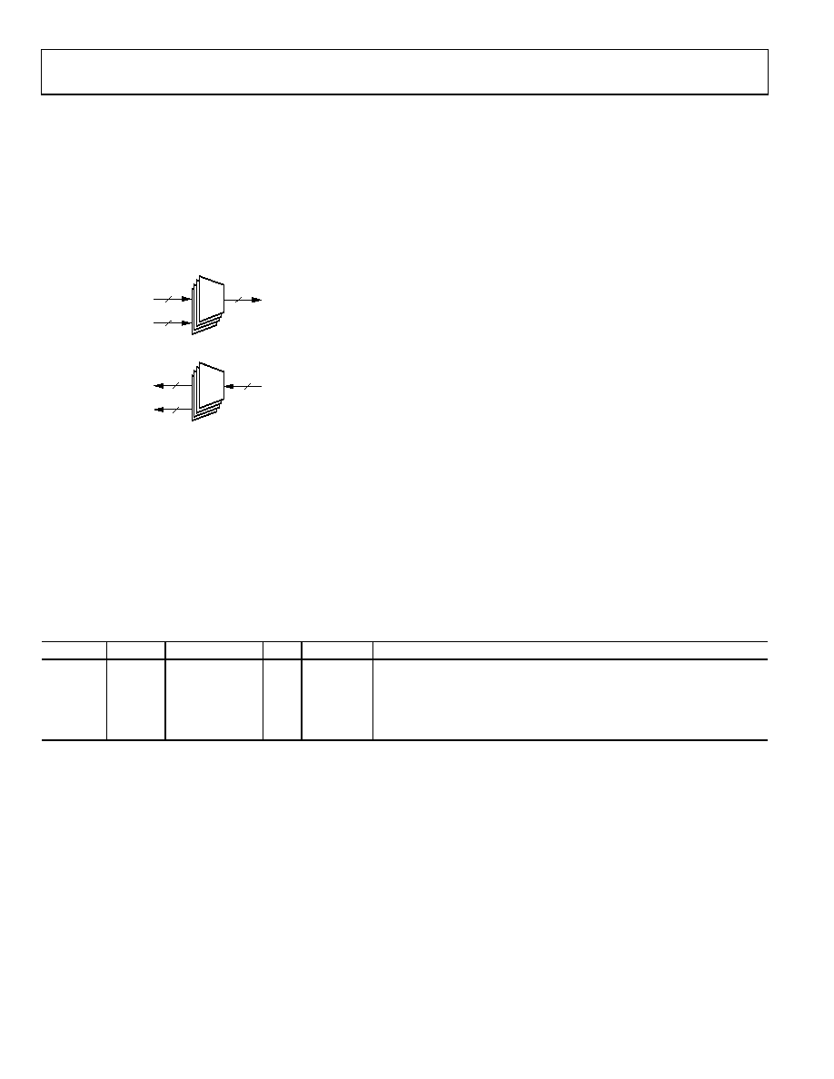
MUX
TXC
RXA
RXB
DEMUX
RXC
TXA
TXB
0
66
46
-0
23
Figure 35. Mux/Demux Paths, Port A to Port C
The part offers extensively programmable transmit output levels
and preemphasis settings as well as squelch or full disable. The
receivers integrate a programmable, multizero transfer function
for aggressive equalization and a programmable loss-of-signal
feature. The AD8158 provides a balanced, high speed switch
core that maintains low lane-to-lane skew while preserving
edge rates.
The I/O on-chip termination resistors are tied to user-settable
supplies for increased flexibility. The AD8158 supports a wide
primary supply range; VCC can be set from 1.8 V to 3.3 V. These
features, together with programmable transmitter output levels,
allow for a wide range of dc- and ac-coupled I/O configurations.
The AD8158 supports several control and configuration modes,
shown in Table 5. The pin control mode offers access to a subset
of the total feature list but allows for a much simplified control
scheme. Table 6 compares the features in all control modes.
The primary advantage of using the serial control interface is
that it allows finer resolution in setting receive equalization,
transmitter preemphasis, loss-of-signal (LOS) behavior, and
output levels.
By default, the AD8158 starts in the pin control mode. Strobing
the RESETb pin sets all on-chip registers to their default values
and uses pins to configure switch connectivity, PE, and EQ
levels. In mixed mode, switch connectivity is still controlled
through the SEL[3:0], LB_[A:C], and BICAST pins. The user
can override PE and EQ settings in mixed mode. In serial
mode, all functions are accessed through registers and the
control pin inputs are ignored, except RESETb.
The AD8158 register set is controlled through a 2-wire I2C
interface. The AD8158 acts only as an I2C slave device. The 7-bit
slave address for the AD8158 I2C interface contains the static
value b1010 for the upper four bits. The lower three bits are
controlled by the input pins, I2C_A[2:0].
Table 5. Control Interface Mode Register
Address
Default
Register Name
Bit
Bit Name
Functionality Description
0x0F
0x00
Control
interface mode
7:2
Reserved
Set to 0.
1:0
Mode[1:0]
00: toggle pin control. Asynchronous control through toggle pins only.
10: mixed control. Switch configuration via toggle pins, register-based
control through the I2C serial interface.
11: serial control. Register-based control through the I2C serial interface.
相关PDF资料 |
PDF描述 |
|---|---|
| AD8159ASVZ | IC MUX/DEMUX QUAD BUFF 100TQFP |
| AD8174ANZ | IC MUX SW W/AMP 250MHZ 14-DIP |
| AD8175ABPZ | IC CROSSPOINT SWITCH TRPL 676BGA |
| AD8176ABPZ | IC VIDEO CROSSPOINT SWIT 676BGA |
| AD8177ABPZ | IC VIDEO CROSSPOINT SWIT 676BGA |
相关代理商/技术参数 |
参数描述 |
|---|---|
| AD8158-EVALZ | 制造商:Analog Devices 功能描述:EVALUATION BOARD - Bulk |
| AD8158XCPZ | 制造商:Analog Devices 功能描述:QUAD-LANE 6.5GBPS 2:1 MUX / 1:2 DEMUX SWITCH 100-PIN LFCSP - Bulk |
| AD8159 | 制造商:AD 制造商全称:Analog Devices 功能描述:3.2 Gbps Quad Buffer Mux/Demux |
| AD8159ASVZ | 功能描述:IC MUX/DEMUX QUAD BUFF 100TQFP RoHS:是 类别:集成电路 (IC) >> 接口 - 专用 系列:XStream™ 特色产品:NXP - I2C Interface 标准包装:1 系列:- 应用:2 通道 I²C 多路复用器 接口:I²C,SM 总线 电源电压:2.3 V ~ 5.5 V 封装/外壳:16-TSSOP(0.173",4.40mm 宽) 供应商设备封装:16-TSSOP 包装:剪切带 (CT) 安装类型:表面贴装 产品目录页面:825 (CN2011-ZH PDF) 其它名称:568-1854-1 |
| AD8159-EVAL-AC | 制造商:Analog Devices 功能描述:EVAL KIT FOR AC-COUPLED EVAL BD - Bulk |
发布紧急采购,3分钟左右您将得到回复。