参数资料
| 型号: | AD817AR |
| 厂商: | Analog Devices Inc |
| 文件页数: | 12/12页 |
| 文件大小: | 0K |
| 描述: | IC OPAMP HS LP 8-SOIC |
| 标准包装: | 98 |
| 应用: | 通用 |
| 电路数: | 1 |
| -3db带宽: | 50MHz |
| 转换速率: | 350 V/µs |
| 电流 - 电源: | 7mA |
| 电流 - 输出 / 通道: | 50mA |
| 电压 - 电源,单路/双路(±): | 5 V ~ 36 V,±2.5 V ~ 18 V |
| 安装类型: | 表面贴装 |
| 封装/外壳: | 8-SOIC(0.154",3.90mm 宽) |
| 供应商设备封装: | 8-SO |
| 包装: | 管件 |
AD817
REV. B
–9–
DRIVING CAPACITIVE LOADS
The internal compensation of the AD817, together with its high
output current drive, permit excellent large signal performance
while driving extremely high capacitive loads.
C
L
1000pF
R
IN
1k
+V
S
TEKTRONIX
P6201 FET
PROBE
HP
PULSE
GENERATOR
50
1k
V
OUT
0.01
F
3.3
F
–V
S
V
IN
TEKTRONIX
7A24
PREAMP
AD817
7
6
3
2
4
0.01
F
3.3
F
Figure 30a. Inverting Amplifier Driving a 1000 pF
Capacitive Load
10
90
100
0%
5V
500ns
5V
100pF
1000pF
Figure 30b. Inverting Amplifier Pulse Response While
Driving Capacitive Loads
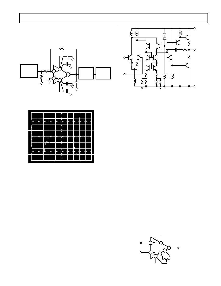
THEORY OF OPERATION
The AD817 is a low cost, wide band, high performance opera-
tional amplifier which effectively drives heavy capacitive or resis-
tive loads. It also provides a constant slew rate, bandwidth and
settling time over its entire specified temperature range.
The AD817 (Figure 31) consists of a degenerated NPN differ-
ential pair driving matched PNPs in a folded-cascode gain stage.
The output buffer stage employs emitter followers in a class AB
amplifier which delivers the necessary current to the load while
maintaining low levels of distortion.
The capacitor, CF, in the output stage mitigates the effect of
capacitive loads. At low frequencies, and with low capacitive
loads, the gain from the compensation node to the output is
very close to unity. In this case, CF is bootstrapped and does not
contribute to the overall compensation capacitance of the device.
As the capacitive load is increased, a pole is formed with the
output impedance of the output stage. This reduces the gain,
and therefore, CF is incompletely bootstrapped. Effectively,
some fraction of CF contributes to the overall compensation
capacitance, reducing the unity gain bandwidth. As the load
capacitance is further increased, the bandwidth continues to fall,
maintaining the stability of the amplifier.
C
F
–IN
+IN
NULL 1
NULL 8
OUTPUT
+VS
–VS
Figure 31. Simplified Schematic
INPUT CONSIDERATIONS
An input protection resistor (RIN in Figure 22) is required in cir-
cuits where the input to the AD817 will be subjected to tran-
sient or continuous overload voltages exceeding the +6 V
maximum differential limit. This resistor provides protection for
the input transistors by limiting their maximum base current.
For high performance circuits, it is recommended that a “bal-
ancing” resistor be used to reduce the offset errors caused by
bias current flowing through the input and feedback resistors.
The balancing resistor equals the parallel combination of RIN
and RF and thus provides a matched impedance at each input
terminal. The offset voltage error will then be reduced by more
than an order of magnitude.
GROUNDING & BYPASSING
When designing high frequency circuits, some special precau-
tions are in order. Circuits must be built with short interconnect
leads. When wiring components, care should be taken to pro-
vide a low resistance, low inductance path to ground. Sockets
should be avoided, since their increased interlead capacitance
can degrade circuit bandwidth.
Feedback resistors should be of low enough value (<1 k
) to
assure that the time constant formed with the inherent stray
capacitance at the amplifier’s summing junction will not limit
performance. This parasitic capacitance, along with the parallel
resistance of RF/RIN, form a pole in the loop transmission which
may result in peaking. A small capacitance (1 pF–5 pF) may be
used in parallel with the feedback resistor to neutralize this effect.
Power supply leads should be bypassed to ground as close as
possible to the amplifier pins. Ceramic disc capacitors of 0.1
F
are recommended.
+V
S
10k
–V
S
AD817
7
3
2
4
8
6
1
V
OS ADJUST
Figure 32. Offset Null Configuration
相关PDF资料 |
PDF描述 |
|---|---|
| AD818AR | IC VIDEO OPAMP 130MHZ LP 8-SOIC |
| AD828AR | IC VIDEO OPAMP DUAL LP 8-SOIC |
| AD829SQ | IC VIDEO OPAMP HS LN 8-CDIP |
| AD8304ARU | IC LOGARITHM CONV 160DB 14-TSSOP |
| AD8305ACPZ-R2 | IC AMP LOG CONV 100DB 16-LFCSP |
相关代理商/技术参数 |
参数描述 |
|---|---|
| AD817AR-EBZ | 功能描述:BOARD EVAL FOR AD817AR RoHS:是 类别:编程器,开发系统 >> 评估演示板和套件 系列:* 标准包装:1 系列:- 主要目的:电信,线路接口单元(LIU) 嵌入式:- 已用 IC / 零件:IDT82V2081 主要属性:T1/J1/E1 LIU 次要属性:- 已供物品:板,电源,线缆,CD 其它名称:82EBV2081 |
| AD817AR-REEL | 功能描述:IC OPAMP LP HS 8-SOIC RoHS:否 类别:集成电路 (IC) >> 线性 - 放大器 - 视频放大器和频缓冲器 系列:- 标准包装:1,000 系列:- 应用:驱动器 输出类型:差分 电路数:3 -3db带宽:350MHz 转换速率:1000 V/µs 电流 - 电源:14.5mA 电流 - 输出 / 通道:60mA 电压 - 电源,单路/双路(±):5 V ~ 12 V,±2.5 V ~ 6 V 安装类型:表面贴装 封装/外壳:20-VFQFN 裸露焊盘 供应商设备封装:20-QFN 裸露焊盘(4x4) 包装:带卷 (TR) |
| AD817AR-REEL7 | 功能描述:IC OPAMP LP HS 8-SOIC RoHS:否 类别:集成电路 (IC) >> 线性 - 放大器 - 视频放大器和频缓冲器 系列:- 标准包装:1,000 系列:- 应用:驱动器 输出类型:差分 电路数:3 -3db带宽:350MHz 转换速率:1000 V/µs 电流 - 电源:14.5mA 电流 - 输出 / 通道:60mA 电压 - 电源,单路/双路(±):5 V ~ 12 V,±2.5 V ~ 6 V 安装类型:表面贴装 封装/外壳:20-VFQFN 裸露焊盘 供应商设备封装:20-QFN 裸露焊盘(4x4) 包装:带卷 (TR) |
| AD817AR-REEL7-DASSAULT | 制造商:Analog Devices 功能描述: |
| AD817ARZ | 功能描述:IC OPAMP LP HS 8-SOIC RoHS:是 类别:集成电路 (IC) >> 线性 - 放大器 - 视频放大器和频缓冲器 系列:- 产品培训模块:Lead (SnPb) Finish for COTS Obsolescence Mitigation Program 标准包装:50 系列:- 应用:TFT-LCD 面板:VCOM 驱动器 输出类型:满摆幅 电路数:1 -3db带宽:35MHz 转换速率:40 V/µs 电流 - 电源:3.7mA 电流 - 输出 / 通道:1.3A 电压 - 电源,单路/双路(±):9 V ~ 20 V,±4.5 V ~ 10 V 安装类型:表面贴装 封装/外壳:8-TSSOP,8-MSOP(0.118",3.00mm 宽)裸露焊盘 供应商设备封装:8-uMax-EP 包装:管件 |
发布紧急采购,3分钟左右您将得到回复。