- 您现在的位置:买卖IC网 > PDF目录11485 > AD8180ARZ (Analog Devices Inc)IC MULTIPLEXER 2X1 8SOIC PDF资料下载
参数资料
| 型号: | AD8180ARZ |
| 厂商: | Analog Devices Inc |
| 文件页数: | 12/12页 |
| 文件大小: | 0K |
| 描述: | IC MULTIPLEXER 2X1 8SOIC |
| 标准包装: | 98 |
| 功能: | 多路复用器 |
| 电路: | 1 x 2:1 |
| 电压电源: | 双电源 |
| 电压 - 电源,单路/双路(±): | ±4 V ~ 6 V |
| 工作温度: | -40°C ~ 85°C |
| 安装类型: | 表面贴装 |
| 封装/外壳: | 8-SOIC(0.154",3.90mm 宽) |
| 供应商设备封装: | 8-SOIC |
| 包装: | 管件 |
| 产品目录页面: | 802 (CN2011-ZH PDF) |
AD8180/AD8182
–9–
REV. B
Picture-in-Picture or Pixel Switching
Many high end display systems require simultaneous display of
two video pictures (from two different sources) on one screen.
Video conferencing is one such example. In this case the remote
site might be displayed as the main picture with a picture of the
local site “inset” for monitoring purposes. The circuit in Fig-
ure 23 could also be used to implement this “picture-in-picture”
application.
Implementing a picture-in-picture algorithm is difficult for
several reasons. Both sources are being displayed simultaneously
(i.e., during the same frame), both sources are in real time, and
both must be synchronized. Figure 24 shows the raster scan-
ning that takes place in all monitors. During every horizontal
scan that includes part of the inset, the source must be switched
twice (i.e., from main to inset and from inset to main). To avoid
screen artifacts, it is critical that switching is clean and fast. The
AD8180 and AD8182, in the above application, switch and
settle to 0.1% accuracy in 14 ns. We quadratically add this
value to the 10 ns settling time of the AD8001, and get an over-
all settling time of 17.2 ns. This yields a sharp, artifact-free
border between the inset and the main video.
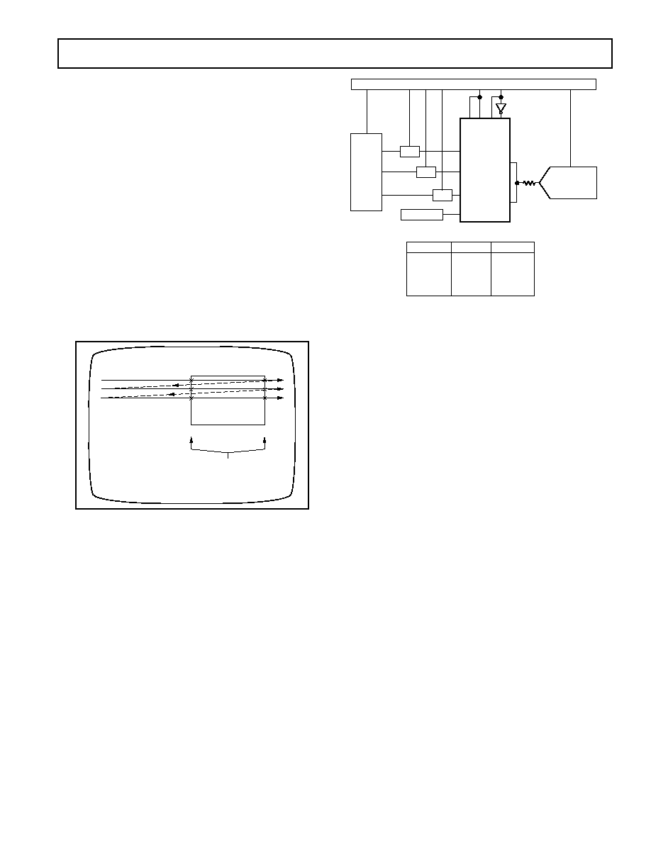
INSET VIDEO
MULTIPLEXER MUST SWITCH
CLEANLY ON EACH CROSSING
MAIN VIDEO
Figure 24. “Picture-in-Picture,” Pixel Switching
Color Document Scanner
Figure 25 shows a block diagram of a Color Document Scan-
ner. Charge Coupled Devices (CCDs) find widespread use in
scanner applications. A monochrome CCD delivers a serial
stream of voltage levels, each level being proportional to the
light shining on that cell. In the case of the color image scanner
shown, there are three output streams, representing red, green
and blue. Interlaced with the stream of voltage levels is a voltage
representing the reset level (or black level) of each cell. A Corre-
lated Double Sampler (CDS) subtracts these two voltages from
each other in order to eliminate the relatively large offsets which
are common with CCDs.
CONTROL AND TIMING
AD876 8/10-BIT
20MSPS
A/D
AD8182
OUT A
OUT B
CDS
REFERENCE
R
G
B
C
D
IN0 A
IN1 A
IN1 B
IN0 B
100
4:1 MUX TRUTH TABLE
SEL A, SEL B
ENA, ENB OUTA, OUTB
0
1
0
1
0
1
IN0A
IN0B
IN1A
IN1B
EN
A
EN
B
SEL
A
SEL
B
Figure 25. Color Document Scanner
The next step in the data acquisition process involves digitizing
the three signal streams. Assuming that the analog to digital
converter chosen has a fast enough sample rate, multiplexing
the three streams into a single ADC is generally more eco-
nomic than using one ADC per channel. In the example
shown, we use the two 2-to-1 multiplexers in the AD8182 to
create a 4-to-1 multiplexer. The enable control pins on the
multiplexers allow the outputs to be wired directly together.
Because of its high bandwidth, the AD8182 is capable of driv-
ing the switched capacitor input stage of the AD876 without
additional buffering. In addition to having the required the
bandwidth, it is necessary to consider the settling time of the
multiplexer. In this case, the ADC has a sample rate of 20 MHz
which corresponds to a sampling period of 50 ns. Typically,
one phase of the sampling clock is used for conversion (i.e., all
levels are held steady) and the other phase is used for switch-
ing and settling to the next channel. Assuming a 50% duty cycle,
the signal chain must settle within 25 ns. With a settling time to
0.1% of 14 ns, the multiplexer easily satisfies this criterion.
In the example shown, the fourth (spare) channel of the
AD8182 is used to measure a reference voltage. This voltage
would probably be measured less frequently than the R, G and
B signals. Multiplexing a reference voltage offers the advantage
that any temperature drift effects caused by the multiplexer
will equally impact the reference voltage and the to-be-
measured signals. If the fourth channel is unused, it is good
design practice to tie this input to ground.
相关PDF资料 |
PDF描述 |
|---|---|
| PIC18LF1320T-I/SO | IC MCU FLASH 4KX16 EEPROM 18SOIC |
| ADG4612BRUZ | IC SWITCH QUAD SPST 16TSSOP |
| VE-B4W-CU-F4 | CONVERTER MOD DC/DC 5.5V 200W |
| VE-B4W-CU-F3 | CONVERTER MOD DC/DC 5.5V 200W |
| ADG1604BRUZ | IC MULTIPLEXER 4X1 14TSSOP |
相关代理商/技术参数 |
参数描述 |
|---|---|
| AD8180ARZ | 制造商:Analog Devices 功能描述:IC ANALOG MULTIPLEXER 2 X 1 ((NW)) 制造商:Analog Devices 功能描述:IC, ANALOG MULTIPLEXER, 2 X 1, SOIC-8 |
| AD8180ARZ-R7 | 功能描述:IC MULTIPLEXER 2X1 8SOIC RoHS:是 类别:集成电路 (IC) >> 接口 - 模拟开关,多路复用器,多路分解器 系列:- 标准包装:1,000 系列:- 功能:多路复用器 电路:1 x 4:1 导通状态电阻:- 电压电源:双电源 电压 - 电源,单路/双路(±):±5V 电流 - 电源:7mA 工作温度:-40°C ~ 85°C 安装类型:表面贴装 封装/外壳:16-SOIC(0.154",3.90mm 宽) 供应商设备封装:16-SOIC 包装:带卷 (TR) |
| AD8180ARZ-RL | 功能描述:IC MULTIPLEXER 2X1 8SOIC RoHS:是 类别:集成电路 (IC) >> 接口 - 模拟开关,多路复用器,多路分解器 系列:- 标准包装:1,000 系列:- 功能:多路复用器 电路:1 x 4:1 导通状态电阻:- 电压电源:双电源 电压 - 电源,单路/双路(±):±5V 电流 - 电源:7mA 工作温度:-40°C ~ 85°C 安装类型:表面贴装 封装/外壳:16-SOIC(0.154",3.90mm 宽) 供应商设备封装:16-SOIC 包装:带卷 (TR) |
| AD8180-EB | 制造商:Analog Devices 功能描述:AD8180 EVALUATION BOARD - Bulk |
| AD8182 | 制造商:AD 制造商全称:Analog Devices 功能描述:750 MHz, 3.8 mA 10 ns Switching Multiplexers |
发布紧急采购,3分钟左右您将得到回复。