- 您现在的位置:买卖IC网 > PDF目录11485 > AD8180ARZ (Analog Devices Inc)IC MULTIPLEXER 2X1 8SOIC PDF资料下载
参数资料
| 型号: | AD8180ARZ |
| 厂商: | Analog Devices Inc |
| 文件页数: | 6/12页 |
| 文件大小: | 0K |
| 描述: | IC MULTIPLEXER 2X1 8SOIC |
| 标准包装: | 98 |
| 功能: | 多路复用器 |
| 电路: | 1 x 2:1 |
| 电压电源: | 双电源 |
| 电压 - 电源,单路/双路(±): | ±4 V ~ 6 V |
| 工作温度: | -40°C ~ 85°C |
| 安装类型: | 表面贴装 |
| 封装/外壳: | 8-SOIC(0.154",3.90mm 宽) |
| 供应商设备封装: | 8-SOIC |
| 包装: | 管件 |
| 产品目录页面: | 802 (CN2011-ZH PDF) |
NOTES
1
ENABLE pin is grounded. IN0 = +1 V dc, IN1 = –1 V dc. SELECT input is driven with 0 V to +5 V pulse. Measure transition time from 50% of the SELECT input value
(+2.5 V) and 10% (or 90%) of the total output voltage transition from IN0 channel voltage (+1 V) to IN1 (–1 V), or vice versa.
2
ENABLE pin is driven with 0 V to +5 V pulse (with 3 ns edges). State of SELECT input determines which channel is activated (i.e., if SELECT = Logic 0, IN0 is selected). Set
IN0 = +1 V dc, IN1 = –1 V dc, and measure transition time from 50% of
ENABLE pulse (+2.5 V) to 90% of the total output voltage change. In Figure 5,
t
OFF is the disable
time,
t
ON is the enable time.
3All inputs are grounded. SELECT input is driven with 0 V to +5 V pulse. The outputs are monitored. Speeding the edges of the SELECT pulse increases the glitch magnitude
due to coupling via the ground plane. Removing the SELECT input termination will lower glitch, as does increasing RL.
4Decreasing R
L lowers the bandwidth slightly. Increasing CL lowers the bandwidth considerably (see Figure 19).
5A resistor (R
S) placed in series with the mux inputs serves to optimize 0.1 dB flatness, but is not required. Increasing output capacitance will increase peaking and reduce band-
width (see Figure 20.)
6Select input which is not being driven (i.e., if SELECT is Logic 1, input activated is IN1); drive all other inputs with V
IN = 0.707 V rms and monitor output at = 5 and 30 MHz.
RL = 1 k
(see Figure 13).
7Mux is disabled (i.e.,
ENABLE = Logic 1) and all inputs are driven simultaneously with V
IN = 0.446 V rms. Output is monitored at = 5 and 30 MHz. R L = 30
to simulate
RON of one enabled mux within a system (see Figure 14). In this mode the output impedance is very high (typ 10 M
), and the signal couples across the package; the load imped-
ance determines the crosstalk.
8Voltage gain decreases for lower values of R
L. The resistive divider formed by the mux enabled output resistance (27
) and R
L causes a gain which decreases as RL decreases
(i.e., the voltage gain is approximately 0.97 V/V (3% gain error) for RL = 1 k
).
9Larger values of R
L provide wider output voltage swings, as well as better gain accuracy. See Note 8.
Specifications subject to change without notice.
AD8180/AD8182
CAUTION
ESD (electrostatic discharge) sensitive device. Electrostatic charges as high as 4000 V readily
accumulate on the human body and test equipment and can discharge without detection.
Although the AD8180/AD8182 feature proprietary ESD protection circuitry, permanent damage
may occur on devices subjected to high energy electrostatic discharges. Therefore, proper ESD
precautions are recommended to avoid performance degradation or loss of functionality.
–3–
REV. B
ABSOLUTE MAXIMUM RATINGS
1
Supply Voltage
. . . . . . . . . . . . . . . . . . . . . . . . . . . . . . . . . 12.6 V
Internal Power Dissipation
2
AD8180 8-Lead Plastic DIP (N) . . . . . . . . . . . . . . . . 1.3 Watts
AD8180 8-Lead Small Outline (R) . . . . . . . . . . . . . . 0.9 Watts
AD8182 14-Lead Plastic DIP (N) . . . . . . . . . . . . . . . 1.6 Watts
AD8182 14-Lead Small Outline (R) . . . . . . . . . . . . . 1.0 Watts
Input Voltage . . . . . . . . . . . . . . . . . . . . . . . . . . . . . . . . . . . . .
±V
S
Output Short Circuit Duration . . . . . Observe Power Derating Curves
Storage Temperature Range
N and R Package . . . . . . . . . . . . . . . . . . . . . . –65
°C to +125°C
Lead Temperature Range (Soldering 10 sec) . . . . . . . . . . +300
°C
NOTES
1Stresses above those listed under Absolute Maximum Ratings may cause perma-
nent damage to the device. This is a stress rating only; functional operation of the
device at these or any other conditions above those indicated in the operational
section of this specification is not implied. Exposure to absolute maximum rating
conditions for extended periods may affect device reliability.
2Specification is for device in free air: 8-Lead Plastic DIP Package:
θ
JA = 90°C/W;
8-Lead SOIC Package:
θ
JA = 155°C/W; 14-Lead Plastic Package: θJA = 75°C/W;
14-Lead SOIC Package:
θ
JA = 120°C/W, where PD = (T J–TA)/θJA.
ORDERING GUIDE
Temperature
Package
Model
Range
Description
Option
AD8180AN
–40
°C to +85°C 8-Lead Plastic DIP
N-8
AD8180AR
–40
°C to +85°C 8-Lead SOIC
SO-8
AD8180AR-REEL
–40
°C to +85°C 13" Reel SOIC
SO-8
AD8180AR-REEL7 –40
°C to +85°C 7" Reel SOIC
SO-8
AD8182AN
–40
°C to +85°C 14-Lead Plastic DIP
N-14
AD8182AR
–40
°C to +85°C 14-Lead Narrow SOIC R-14
AD8182AR-REEL
–40
°C to +85°C 13" Reel SOIC
R-14
AD8182AR-REEL7 –40
°C to +85°C 7" Reel SOIC
R-14
AD8180-EB
Evaluation Board
AD8182-EB
Evaluation Board
MAXIMUM POWER DISSIPATION
The maximum power that can be safely dissipated by the
AD8180 and AD8182 is limited by the associated rise in junc-
tion temperature. The maximum safe junction temperature for
plastic encapsulated devices is determined by the glass transition
temperature of the plastic, approximately +150
°C. Exceeding
this limit temporarily may cause a shift in parametric perfor-
mance due to a change in the stresses exerted on the die by the
package. Exceeding a junction temperature of +175
°C for an
extended period can result in device failure.
While the AD8180 and AD8182 are internally short circuit
protected, this may not be sufficient to guarantee that the maxi-
mum junction temperature (+150
°C) is not exceeded under all
conditions. To ensure proper operation, it is necessary to observe
the maximum power derating curves shown in Figures 2 and 3.
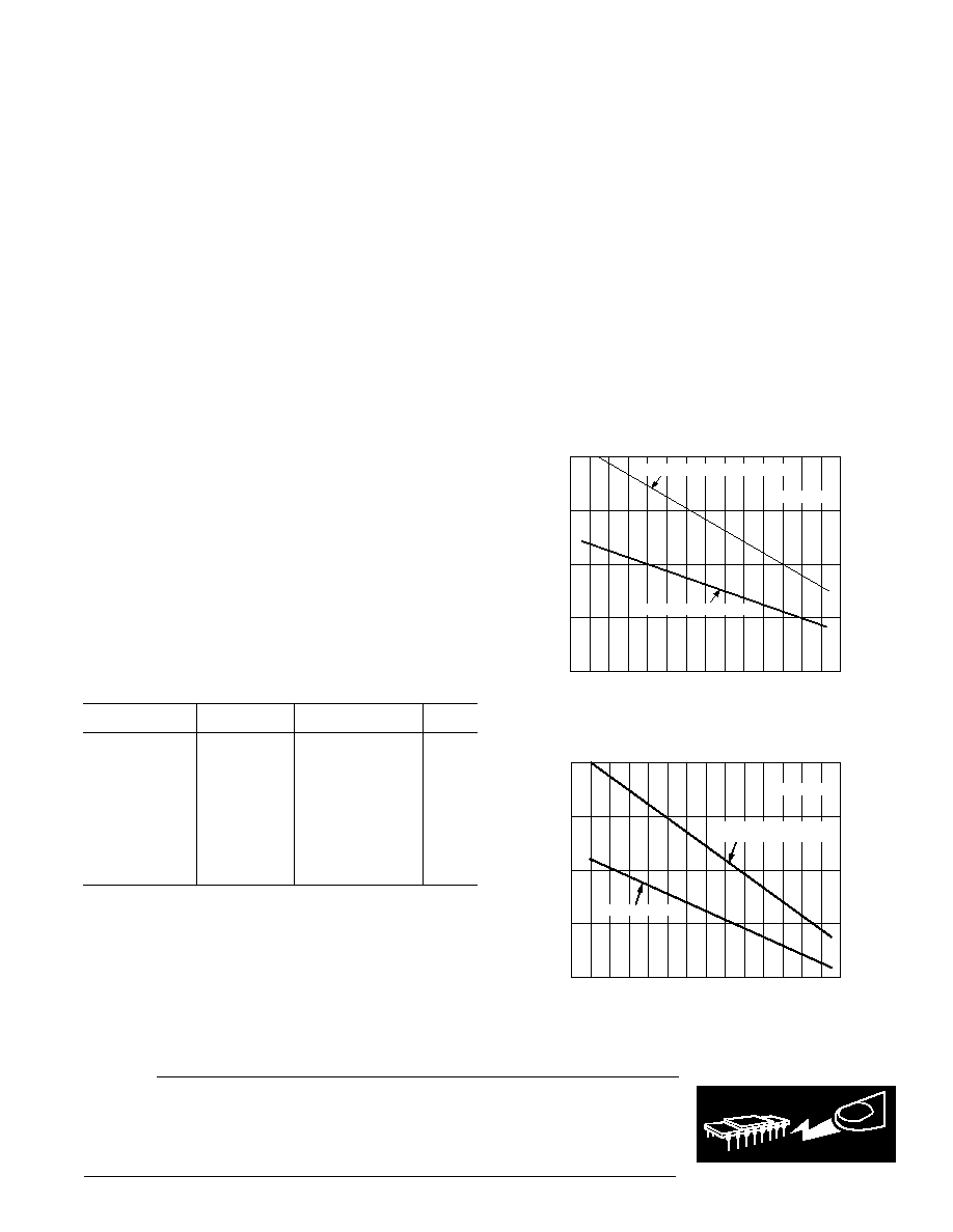
MAXIMUM
POWER
DISSIPATION
–
Watts
AMBIENT TEMPERATURE – C
2.0
1.5
0
–50
90
–40 –30 –20 –10
0
10 20
30
50 60
70 80
40
1.0
0.5
8-LEAD PLASTIC DIP PACKAGE
8-LEAD SOIC PACKAGE
TJ = +150 C
Figure 2. AD8180 Maximum Power Dissipation vs.
Temperature
AMBIENT TEMPERATURE – C
2.5
2.0
0.5
–50
90
–40
MAXIMUM
POWER
DISSIPATION
–
Watts
–30 –20 –10 0
10 20
30 40 50
60
80
1.5
1.0
70
14-LEAD SOIC
14-LEAD
PLASTIC DIP PACKAGE
TJ = +150 C
Figure 3. AD8182 Maximum Power Dissipation vs.
Temperature
WARNING!
ESD SENSITIVE DEVICE
相关PDF资料 |
PDF描述 |
|---|---|
| PIC18LF1320T-I/SO | IC MCU FLASH 4KX16 EEPROM 18SOIC |
| ADG4612BRUZ | IC SWITCH QUAD SPST 16TSSOP |
| VE-B4W-CU-F4 | CONVERTER MOD DC/DC 5.5V 200W |
| VE-B4W-CU-F3 | CONVERTER MOD DC/DC 5.5V 200W |
| ADG1604BRUZ | IC MULTIPLEXER 4X1 14TSSOP |
相关代理商/技术参数 |
参数描述 |
|---|---|
| AD8180ARZ | 制造商:Analog Devices 功能描述:IC ANALOG MULTIPLEXER 2 X 1 ((NW)) 制造商:Analog Devices 功能描述:IC, ANALOG MULTIPLEXER, 2 X 1, SOIC-8 |
| AD8180ARZ-R7 | 功能描述:IC MULTIPLEXER 2X1 8SOIC RoHS:是 类别:集成电路 (IC) >> 接口 - 模拟开关,多路复用器,多路分解器 系列:- 标准包装:1,000 系列:- 功能:多路复用器 电路:1 x 4:1 导通状态电阻:- 电压电源:双电源 电压 - 电源,单路/双路(±):±5V 电流 - 电源:7mA 工作温度:-40°C ~ 85°C 安装类型:表面贴装 封装/外壳:16-SOIC(0.154",3.90mm 宽) 供应商设备封装:16-SOIC 包装:带卷 (TR) |
| AD8180ARZ-RL | 功能描述:IC MULTIPLEXER 2X1 8SOIC RoHS:是 类别:集成电路 (IC) >> 接口 - 模拟开关,多路复用器,多路分解器 系列:- 标准包装:1,000 系列:- 功能:多路复用器 电路:1 x 4:1 导通状态电阻:- 电压电源:双电源 电压 - 电源,单路/双路(±):±5V 电流 - 电源:7mA 工作温度:-40°C ~ 85°C 安装类型:表面贴装 封装/外壳:16-SOIC(0.154",3.90mm 宽) 供应商设备封装:16-SOIC 包装:带卷 (TR) |
| AD8180-EB | 制造商:Analog Devices 功能描述:AD8180 EVALUATION BOARD - Bulk |
| AD8182 | 制造商:AD 制造商全称:Analog Devices 功能描述:750 MHz, 3.8 mA 10 ns Switching Multiplexers |
发布紧急采购,3分钟左右您将得到回复。