参数资料
| 型号: | AD8203YRZ-RL |
| 厂商: | Analog Devices Inc |
| 文件页数: | 6/20页 |
| 文件大小: | 0K |
| 描述: | IC AMP DIFF 60KHZ 8SOIC |
| 标准包装: | 2,500 |
| 放大器类型: | 差分 |
| 电路数: | 1 |
| 转换速率: | 0.330 V/µs |
| 增益带宽积: | 60kHz |
| 电流 - 输入偏压: | 40nA |
| 电压 - 输入偏移: | 1000µV |
| 电流 - 电源: | 250µA |
| 电压 - 电源,单路/双路(±): | 3.5 V ~ 12 V |
| 工作温度: | -40°C ~ 125°C |
| 安装类型: | 表面贴装 |
| 封装/外壳: | 8-SOIC(0.154",3.90mm 宽) |
| 供应商设备封装: | 8-SO |
| 包装: | 带卷 (TR) |
AD8203
Data Sheet
Rev. D | Page 14 of 20
APPLICATIONS
The AD8203 difference amplifier is intended for applications
that require extracting a small differential signal in the presence
of large common-mode voltages. The input resistance is nominally
320 k, and the device can tolerate common-mode voltages
higher than the supply voltage and lower than ground.
The open collector output stage sources current to within
20 mV of ground and to within 200 mV of VS.
CURRENT SENSING
High Line, High Current Sensing
Basic automotive applications making use of the large common-
mode range are shown in Figure 2 and Figure 3. The capability
of the device to operate as an amplifier in primary battery sup-
ply circuits is shown in Figure 2. Figure 3 illustrates the ability
of the device to withstand voltages below system ground.
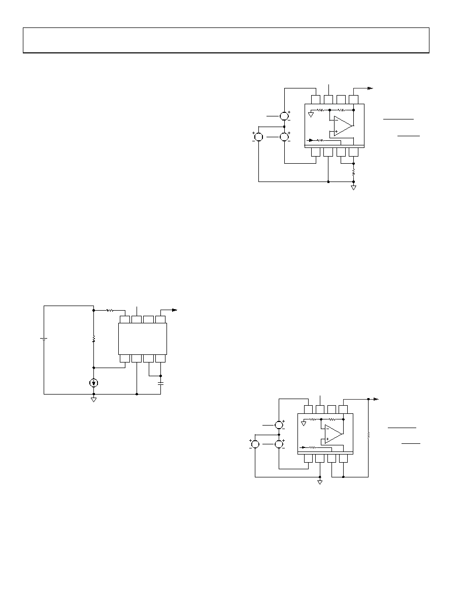
Low Current Sensing
The AD8203 is also used in low current sensing applications,
such as the 4 to 20 mA current loop shown in Figure 42. In such
applications, the relatively large shunt resistor can degrade the
common-mode rejection. Adding a resistor of equal value on the
low impedance side of the input corrects this error.
5V
OUTPUT
10
1%
10
1%
NC = NO CONNECT
+
GND
NC
–IN
+IN
A1
+VS
A2
OUT
AD8203
05013-015
Figure 42. 4 to 20 mA Current Loop Receiver
GAIN ADJUSTMENT
The default gain of the preamplifier and buffer are ×7 and ×2,
respectively, resulting in a composite gain of ×14. With the
addition of external resistor(s) or trimmer(s), the gain can be
lowered, raised, or finely calibrated.
Gains Less Than 14
Since the preamplifier has an output resistance of 100 k, an
external resistor connected from Pin 3 and Pin 4 to GND
decreases the gain by a factor REXT/(100 k + REXT), as shown
10k
10k
100k
A2
A1
GND
–IN
OUT
+VS
NC
+IN
AD8203
OUT
+VS
REXT
VCM
VDIFF
2
GAIN =
14REXT
REXT + 100k
REXT = 100k
GAIN
14 – GAIN
VDIFF
2
NC = NO CONNECT
05013-016
Figure 43. Adjusting for Gains < 14
The overall bandwidth is unaffected by changes in gain by using
this method, although there may be a small offset voltage due to
the imbalance in source resistances at the input to the buffer.
This can often be ignored, but if desired, it can be nulled by
inserting a resistor equal to 100 k minus the parallel sum of
REXT and 100 k, in series with Pin 4. For example, with
REXT = 100 k (yielding a composite gain of ×7), the optional
offset nulling resistor is 50 k.
Gains Greater Than 14
Connecting a resistor from the output of the buffer amplifier to
its noninverting input, as shown in Figure 44, increases the
gain. The gain is now multiplied by the factor REXT/(REXT
100 k); for example, the gain is doubled for REXT = 200 k.
Overall gains as high as 50 are achievable this way. Note that the
accuracy of the gain becomes critically dependent on the
resistor value at high gains. Also, the effective input offset
voltage at Pin 1 and Pin 8 (about six times the actual offset of
A1) limits the part’s use in high gain, dc-coupled applications.
10k
10k
100k
A2
A1
GND
–IN
OUT
+VS
NC
+IN
AD8203
OUT
+VS
REXT
VCM
VDIFF
2
GAIN =
14REXT
REXT – 100k
REXT = 100k
GAIN
GAIN – 14
VDIFF
2
NC = NO CONNECT
05013-017
Figure 44. Adjusting for Gains > 14
相关PDF资料 |
PDF描述 |
|---|---|
| LTC6912HGN-1#PBF | IC PGA DIGITAL R-R DUAL 16SSOP |
| AD8206YRZ-REEL | IC AMP DIFF 8SOIC |
| TMM-113-01-S-S | CONN HEADER 13POS SNGL 2MM T/H |
| MMB21-0141K1 | CONN RACK/PANEL 14POS 5A |
| TMM-114-01-S-S | CONN HEADER 14POS SNGL 2MM T/H |
相关代理商/技术参数 |
参数描述 |
|---|---|
| AD8205 | 制造商:AD 制造商全称:Analog Devices 功能描述:Single-Supply 42 V System Difference Amplifier |
| AD8205AR | 制造商:Analog Devices 功能描述:- Bulk |
| AD8205WHRZ | 制造商:Analog Devices 功能描述:42VSNGLSUPPLYDIFFAMP - Rail/Tube 制造商:Analog Devices 功能描述:IC OPAMP DIFF 50KHZ 8SOIC 制造商:Analog Devices 功能描述:42V Sngl Supply Diff Amp |
| AD8205WHRZ-RL | 制造商:Analog Devices 功能描述:42VSNGLSUPPLYDIFFAMP - Tape and Reel 制造商:Analog Devices 功能描述:IC OPAMP DIFF 50KHZ 8SOIC 制造商:Analog Devices 功能描述:42V Sngl Supply Diff Amp |
| AD8205WYRZ | 功能描述:IC AMP DIFF 42V SGL 8SOIC RoHS:是 类别:集成电路 (IC) >> Linear - Amplifiers - Instrumentation 系列:- 标准包装:100 系列:- 放大器类型:通用 电路数:1 输出类型:- 转换速率:0.2 V/µs 增益带宽积:- -3db带宽:- 电流 - 输入偏压:100pA 电压 - 输入偏移:30µV 电流 - 电源:380µA 电流 - 输出 / 通道:- 电压 - 电源,单路/双路(±):±2 V ~ 18 V 工作温度:0°C ~ 70°C 安装类型:表面贴装 封装/外壳:8-SOIC(0.154",3.90mm 宽) 供应商设备封装:8-SO 包装:管件 |
发布紧急采购,3分钟左右您将得到回复。