- 您现在的位置:买卖IC网 > PDF目录6074 > AD8220ARMZ-R7 (Analog Devices Inc)IC AMP INST JFET R-R 15MA 8MSOP PDF资料下载
参数资料
| 型号: | AD8220ARMZ-R7 |
| 厂商: | Analog Devices Inc |
| 文件页数: | 11/28页 |
| 文件大小: | 0K |
| 描述: | IC AMP INST JFET R-R 15MA 8MSOP |
| 产品培训模块: | Power Line Monitoring Top Five Instrumentation Amplifier Problems Instrumentation Amplifiers Performance |
| 设计资源: | Fully Isolated Input Module Based on AD7793, ADuM5401, and a High Performance In-Amp (CN0067) |
| 标准包装: | 1 |
| 放大器类型: | 仪表 |
| 电路数: | 1 |
| 输出类型: | 满摆幅 |
| 转换速率: | 2 V/µs |
| -3db带宽: | 1.5MHz |
| 电流 - 输入偏压: | 25pA |
| 电压 - 输入偏移: | 250µV |
| 电流 - 电源: | 750µA |
| 电流 - 输出 / 通道: | 15mA |
| 电压 - 电源,单路/双路(±): | 4.5 V ~ 36 V,±2.25 V ~ 18 V |
| 工作温度: | -40°C ~ 85°C |
| 安装类型: | 表面贴装 |
| 封装/外壳: | 8-TSSOP,8-MSOP(0.118",3.00mm 宽) |
| 供应商设备封装: | 8-MSOP |
| 包装: | 标准包装 |
| 产品目录页面: | 771 (CN2011-ZH PDF) |
| 其它名称: | AD8220ARMZ-R7DKR |
第1页第2页第3页第4页第5页第6页第7页第8页第9页第10页当前第11页第12页第13页第14页第15页第16页第17页第18页第19页第20页第21页第22页第23页第24页第25页第26页第27页第28页
AD8220
Rev. B | Page 19 of 28
THEORY OF OPERATION
Q2
Q1
NODE A
NODE B
NODE C
NODE D
VB
C1
C2
A1
A2
–VS
+VS
–VS
J1
+IN
VPINCH
+VS
–VS
J2
–IN
VPINCH
+VS
–VS
RG
+VS
–VS
20k
+VS
–VS
+VS
–VS
REF
OUTPUT
A3
NODE E
NODE F
I
R2
24.7k
R1
24.7k
03
57
9-
00
6
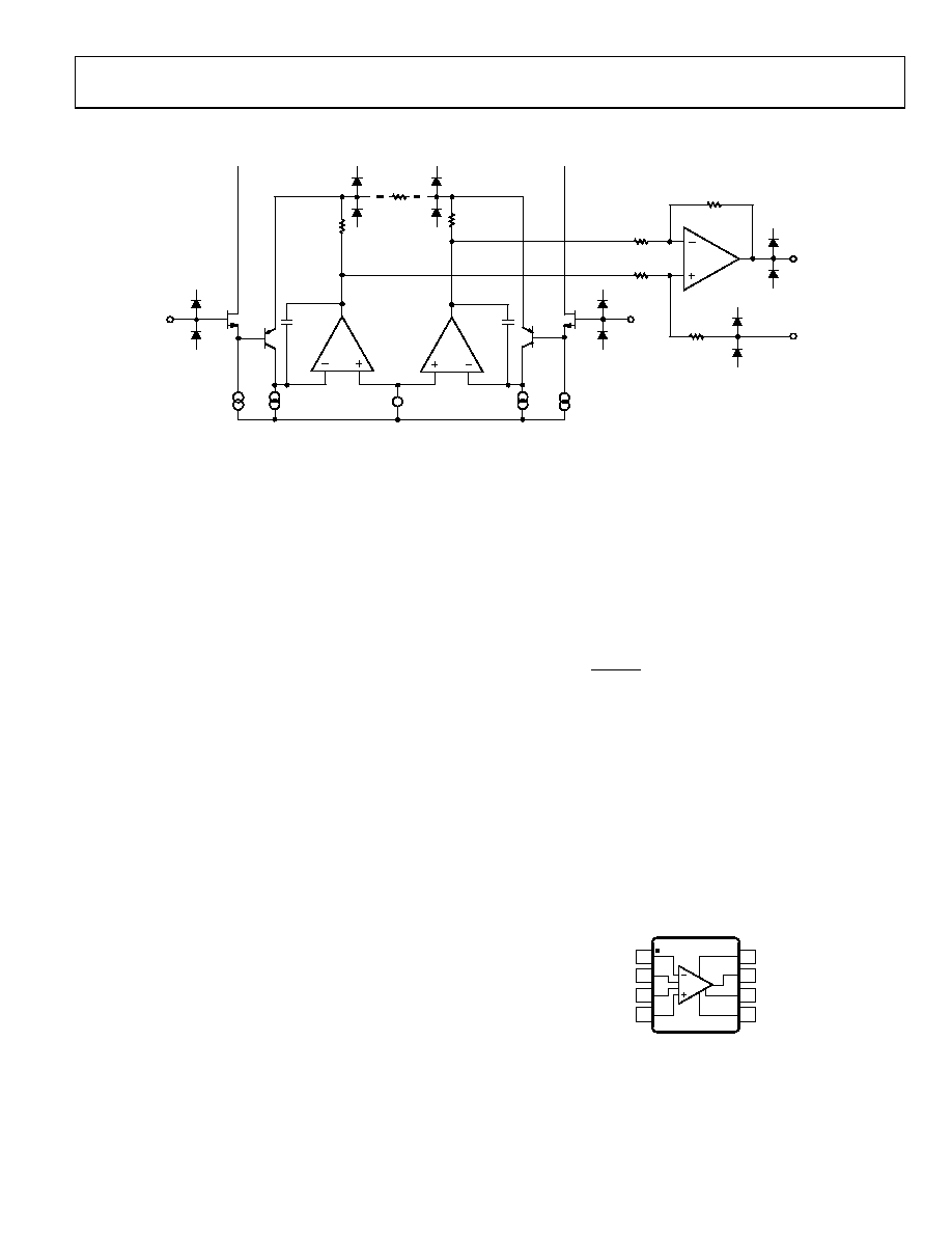
Figure 55. Simplified Schematic
The AD8220 is a JFET input, monolithic instrumentation amplifier
based on the classic 3-op amp topology (see Figure 55). Input
Transistor J1 and Input Transistor J2 are biased at a fixed current so
that any input signal forces the output voltages of A1 and A2 to
change accordingly; the input signal creates a current through RG
that flows in R1 and R2 such that the outputs of A1 and A2 provide
the correct, gained signal. Topologically, J1, A1, and R1 and J2, A2,
and R2 can be viewed as precision current feedback amplifiers that
have a gain bandwidth of 1.5 MHz. The common-mode voltage
and amplified differential signal from A1 and A2 are applied to a
difference amplifier that rejects the common-mode voltage but
amplifies the differential signal. The difference amplifier employs
20 kΩ laser-trimmed resistors that result in an in-amp with gain
error less than 0.04%. New trim techniques were developed to
ensure that CMRR exceeds 86 dB (G = 1).
Using JFET transistors, the AD8220 offers an extremely high
input impedance, extremely low bias currents of 10 pA
maximum, a low offset current of 0.6 pA maximum, and no
input bias current noise. In addition, input offset is less than
125 μV and drift is less than 5 μV/°C. Ease of use and robustness
were considered. A common problem for instrumentation
amplifiers is that at high gains, when the input is overdriven,1
an excessive milliampere input bias current can result and the
output can undergo phase reversal. The AD8220 has none of
these problems; its input bias current is limited to less than
10 μA, and the output does not phase reverse under overdrive
fault conditions.
1 Overdriving the input at high gains refers to when the input signal is within
the supply voltages but the amplifier cannot output the gained signal. For
example, at a gain of 100, driving the amplifier with 10 V on ±15 V constitutes
overdriving the inputs since the amplifier cannot output 100 V.
The AD8220 has extremely low load-induced nonlinearity. All
amplifiers that comprise the AD8220 have rail-to-rail output
capability for enhanced dynamic range. The input of the AD8220
can amplify signals with wide common-mode voltages even
slightly lower than the negative supply rail. The AD8220 operates
over a wide supply voltage range. It can operate from either a
single +4.5 V to +36 V supply or a dual ±2.25 V to ±18 V. The
transfer function of the AD8220 is
G
R
G
kΩ
49.4
1
Users can easily and accurately set the gain using a single,
standard resistor. Because the input amplifiers employ a current
feedback architecture, the AD8220 gain-bandwidth product
increases with gain, resulting in a system that does not suffer as
much bandwidth loss as voltage feedback architectures at higher
gains. A unique pinout enables the AD8220 to meet a CMRR
specification of 80 dB through 5 kHz (G = 1). The balanced
pinout, shown in Figure 56, reduces parasitics that adversely
affect CMRR performance. In addition, the new pinout
simplifies board layout because associated traces are grouped
together. For example, the gain setting resistor pins are adjacent
to the inputs, and the reference pin is next to the output.
TOP VIEW
(Not to Scale)
03
57
9-
00
5
–IN
1
RG 2
RG 3
+IN
4
+VS
8
VOUT
7
REF
6
–VS
5
AD8220
Figure 56. Pin Configuration
相关PDF资料 |
PDF描述 |
|---|---|
| KD1205PFB1 H | FAN 12VDC 50X10.5MM 1.6W 11.4CFM |
| KD1205PFB3 H | FAN 12VDC 50X10.5MM .8W 8.0CFM |
| AD8651ARZ | IC OPAMP VF CMOS 50MHZ LN 8SOIC |
| 0324.125HXP | FUSE CERM 250V FST AXL 3AB .125A |
| AD8619ARUZ | IC OPAMP GP R-R CMOS LN 14TSSOP |
相关代理商/技术参数 |
参数描述 |
|---|---|
| AD8220ARMZ-RL | 功能描述:IC AMP INST JFET R-R 15MA 8MSOP RoHS:是 类别:集成电路 (IC) >> Linear - Amplifiers - Instrumentation 系列:- 标准包装:100 系列:- 放大器类型:通用 电路数:1 输出类型:- 转换速率:0.2 V/µs 增益带宽积:- -3db带宽:- 电流 - 输入偏压:100pA 电压 - 输入偏移:30µV 电流 - 电源:380µA 电流 - 输出 / 通道:- 电压 - 电源,单路/双路(±):±2 V ~ 18 V 工作温度:0°C ~ 70°C 安装类型:表面贴装 封装/外壳:8-SOIC(0.154",3.90mm 宽) 供应商设备封装:8-SO 包装:管件 |
| AD8220BRMZ | 功能描述:IC AMP INST JFET R-R 15MA 8MSOP RoHS:是 类别:集成电路 (IC) >> Linear - Amplifiers - Instrumentation 系列:- 标准包装:2,500 系列:- 放大器类型:通用 电路数:4 输出类型:- 转换速率:0.6 V/µs 增益带宽积:1MHz -3db带宽:- 电流 - 输入偏压:45nA 电压 - 输入偏移:2000µV 电流 - 电源:1.4mA 电流 - 输出 / 通道:40mA 电压 - 电源,单路/双路(±):3 V ~ 32 V,±1.5 V ~ 16 V 工作温度:0°C ~ 70°C 安装类型:表面贴装 封装/外壳:14-TSSOP(0.173",4.40mm 宽) 供应商设备封装:14-TSSOP 包装:带卷 (TR) 其它名称:LM324ADTBR2G-NDLM324ADTBR2GOSTR |
| AD8220BRMZ-R7 | 功能描述:IC AMP INST JFET R-R 15MA 8MSOP RoHS:是 类别:集成电路 (IC) >> Linear - Amplifiers - Instrumentation 系列:- 标准包装:50 系列:- 放大器类型:J-FET 电路数:2 输出类型:- 转换速率:13 V/µs 增益带宽积:3MHz -3db带宽:- 电流 - 输入偏压:65pA 电压 - 输入偏移:3000µV 电流 - 电源:1.4mA 电流 - 输出 / 通道:- 电压 - 电源,单路/双路(±):7 V ~ 36 V,±3.5 V ~ 18 V 工作温度:-40°C ~ 85°C 安装类型:通孔 封装/外壳:8-DIP(0.300",7.62mm) 供应商设备封装:8-PDIP 包装:管件 |
| AD8220BRMZ-RL | 功能描述:IC AMP INST JFET R-R 15MA 8MSOP RoHS:是 类别:集成电路 (IC) >> Linear - Amplifiers - Instrumentation 系列:- 标准包装:50 系列:- 放大器类型:J-FET 电路数:2 输出类型:- 转换速率:13 V/µs 增益带宽积:3MHz -3db带宽:- 电流 - 输入偏压:65pA 电压 - 输入偏移:3000µV 电流 - 电源:1.4mA 电流 - 输出 / 通道:- 电压 - 电源,单路/双路(±):7 V ~ 36 V,±3.5 V ~ 18 V 工作温度:-40°C ~ 85°C 安装类型:通孔 封装/外壳:8-DIP(0.300",7.62mm) 供应商设备封装:8-PDIP 包装:管件 |
| AD8220-EVAL | 制造商:AD 制造商全称:Analog Devices 功能描述:JFET Input Instrumentation Amplifier with Rail-to-Rail Output in MSOP Package |
发布紧急采购,3分钟左右您将得到回复。